
Electronics News
Archive : 1 December 2015 год
 Researchers from North Carolina State University have discovered a new phase of solid carbon, called Q-carbon. It is said to be distinct from known phases of graphite and diamond. They have also developed a technique for using Q-carbon to make diamond-related structures at room temperature and at ambient atmospheric pressure in air.
Q-carbon - the third solid phase of carbon, alongside diamond and graphite – and is ferromagnetic, which other solid forms of carbon are not. It is also claimed to be harder than diamond and glows when exposed to even low levels of energy.
"Q-carbon's strength and low work-function - its willingness to release electrons - make it very promising for developing new electronic display technologies," said Jay Narayan, the John C. C. Fan Distinguished Chair Professor of Materials Science and Engineering at NC State.
But Q-carbon can also be used to create single-crystal diamond objects. To do this researchers start with a substrate, such as such as sapphire, glass or a plastic polymer. The substrate is then coated with amorphous carbon, an elemental carbon that, unlike graphite or diamond, does not have a regular, well-defined crystalline structure. The carbon is then hit with a single laser pulse lasting approximately 200ns. During this pulse, the temperature of the carbon is raised to around 3727°C and then rapidly cooled. This operation takes place at one atmosphere: the same pressure as the surrounding air.
The end result is a film of Q-carbon. The researchers can control the process to make films between 20 and 500nm thick. By using different substrates and changing the duration of the laser pulse, the researchers can also control how quickly the carbon cools, creating diamond structures within the Q-carbon.
"We can create diamond nanoneedles or microneedles, nanodots, or large-area diamond films, with applications for drug delivery, industrial processes and for creating high-temperature switches and power electronics," Narayan said. "These diamond objects have a single-crystalline structure, making them stronger than polycrystalline materials. And it is all done at room temperature and at ambient atmosphere. So, not only does this allow us to develop new applications, but the process itself is relatively inexpensive."
Narayan continued: "We can make Q-carbon films, and we're learning its properties, but we are still in the early stages of understanding how to manipulate it. We know a lot about diamond, so we can make diamond nanodots. We don't yet know how to make Q-carbon nanodots or microneedles. That's something we're working on."
Author
Tom Austin-Morgan
Source: www.newelectronics.co.uk
 PENTA – a new EUREKA cluster – has been launched with the ambition to stimulate up to €1.5billion of investment in research and development in the electronics components and systems industry. According to PENTA, it has already received guarantees for the first €500,000 of funding.
The organisation says it has been established to support the vision and strategy outlined by the Electronic Leaders Group (ELG). This 11 strong group was set up in 2013 in order to respond to the challenge laid down by Neelie Kroes, at the time vice president of the European Commission, for Europe to capture 20% of global semiconductor production within a decade. ELG produced its response in February 2014, suggesting Europe should focus on areas where it is strong, but also on emerging high growth areas, such as the IoT.
PENTA will run for five years, looking to complement and enhance the collaboration and contribution of the European industrial and technology organisations in the ECSEL Joint Technology Initiative. Initially focused on technology underpinning automotive, health and industrial productivity, PENTA says it will also address projects of common interest to industry and public authorities.
Outlining its vision, PENTA says industry needs a programme that is dedicated to micro and nanoelectronics, but which is complementary to and differentiated from ECSEL. It aims to be flexible and agile while taking advantage of European capabilities, with a special emphasis on enabling SMEs to bring new capability into the micro and nanoelectronics based systems markets.
Author
Graham Pitcher
Source: www.newelectronics.co.uk
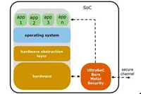 In a move designed to enhanced security, UltraSOC has extended its on chip monitoring and analytics capability to embedded products ranging from embedded IoT devices to enterprise systems.
Called Bare Metal Security, the features are implemented as hardware running underneath the operating system. According to the company, the features are non intrusive and robust, even if the host system’s security measures are compromised. UltraSOC says Bare Metal Security features will typically complement conventional security measures, rather than replace them.
Rupert Baines, UltraSoC’s CEO said: “Our Bare Metal Security tools complement traditional security mechanisms, adding protection against both malicious attacks and against inadvertent malfunctions.”
Bare Metal Security uses UltraSoC monitors to watch for unexpected behaviour, such as suspicious memory accesses or processor activity, at hardware speed. The orthogonal on-chip hardware infrastructure is independent of main system functionality and software, meaning system performance is not impacted. The company notes that it will be very difficult for an attacker to subvert or tamper with the approach. Because Bare Metal Security features also provide visibility of the whole system, it will be difficult to camouflage or hide an attack
Author
Graham Pitcher
Source: www.newelectronics.co.uk
 Imagination Technologies has launched the Creator Ci40 development kit, designed to support the development of smart home, IoT and other connected products. However, according to the developer, the kit also has the ability to be used as a high speed wireless router.
The board runs Linux and Brillo and Imagination says Creator has been selected by Google to be part of its Brillo golden reference programme.
The kit is designed around the cXT200, a dual core chip that has been optimised for IoT and networking applications. Alongside high performance – the dual MIPS cores run at up to 550MHz – the chip boasts a feature set aimed at low power consumption. The board features 256Mbyte of DDR3 SDRAM, 512Mbyte of NAND flash and a microSD card slot.
A full wireless connectivity package is said to be available, including: IEEE802.11ac 2x2 Wi-Fi, Bluetooth Classic and Low Energy, and IEEE802.15.4. There is also an RJ45 Ethernet port and a Micro USB 2.0 OTG port.
The Creator Ci40 IoT kit comes with two battery powered 6LoWPAN Clicker expansion boards and three Click companion boards. Clicker boards are compact development boards based on the mikroBUS socket. When used with the Click boards, they are said to provide a quick way to prototype and build standalone gadgets that connect to the Creator Ci40 IoT hub using low power wireless standards.
Author
Graham Pitcher
Source: www.newelectronics.co.uk