
Electronics News
Archive : 8 December 2015 год
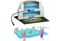 Researchers at Columbia University in New York say they have adenosine triphosphate (ATP) to power an integrated circuit. The team coupled a conventional CMOS circuit with an artificial lipid bilayer membrane containing ATP powered ion pumps and say this could open the door to creating systems that contain biological and solid-state components.
“In combining a biological electronic device with CMOS, we will be able to create new systems not possible with either technology alone,” said Professor Ken Shepard. “We are excited at the prospect of expanding the palette of active devices that will have new functions, such as harvesting energy from ATP, as was done here, or recognising specific molecules, giving chips the potential to taste and smell.”
In living systems, energy is stored in potentials across lipid membranes, with ATP transporting the energy from where it is generated to where it is consumed. Prof Shepard’s team packaged a CMOS circuit with an ATP harvesting ‘biocell’. In the presence of ATP, the system pumped ions across the membrane, producing an electrical potential which was harvested by the chip.
The ability to build a system that combines the power of solid state electronics with the capabilities of biological components has great promise, says the team. “You need a bomb-sniffing dog now,” Prof Shepard noted, “but if you can take just the part of the dog that is useful – the molecules that are doing the sensing – we wouldn’t need the whole animal.”
According to the team, the work provides new insight into a generalised circuit model. “We will now be looking at how to scale the system down,” Prof Shepard concluded.
Author
Graham Pitcher
Source: www.newelectronics.co.uk
 CEA-Leti has announced what it calls preliminary steps for demonstrating a quantum bit – or qubit – in a process usjng a silicon on insulator (SoI) CMOS platform.
According to the French R&D organisation, the leading solid state approach for treating quantum information uses superconducting qubits, but it says other approaches are available. These include semiconductor spin qubits, previously demonstrated using III-V materials, which have a limited ‘lifetime’ due to coupling between the electron spin and the nuclear spins of the III-V elements.
Recently, work on isotopically purified silicon 28 has proved an attractive candidate, but CEA-Leti says the main challenge is to define an elementary cell compatible with circuit upscaling to hundreds of qubits.
Working with Inac, Leti is investigating an SoI approach developed originally for CMOS VLSI circuits. In this approach, quantum dots are created beneath the gates of n-type (respectively p-type) field effect transistors, which are designed to operate in the ‘few electron’ (respectively ‘few hole’) regime at temperatures of less than 0.1K.
According to the partners, they have developed a process for mastering control of the operation of both types of devices using Leti’s SOI nanowire FET technology. The team has demonstrated the co-integration and successful operation of quantum objects with standard ring oscillators on 300mm SOI substrates.
“This technology has acquired a certain degree of robustness and we aim at using it, with very minor modifications, to demonstrate qubits co-integrated with their control electronics,” said Louis Hutin, scientific staff. “This co-integration success represents a critical asset for the eventual design of a quantum computer.”
Meanwhile, the researchers say a qubit demonstration could be on the near horizon. The next step for the teams is to demonstrate a few coupled qubits and to develop a strategy for long range coupling of th
Author
Graham Pitcher
Source: www.newelectronics.co.uk
 Researchers at the Fraunhofer Institute have developed an energy storage device which is said to be significantly more cost-effective over the entire life cycle of a battery than previous approaches.
Batteries for electric vehicles are, in general, monolithic blocks accommodating individual cells and the necessary technology. While all cells should, in theory, be able to save the same amount of energy, this is not the case in practice. The team says this is problematic; since cells are connected in series, the battery is only as strong as its weakest cell. If this cell is ‘empty’, the energy in the other battery cells does not help and when a cell is defective, the vehicle stops functioning.
Researchers at the Fraunhofer Institute for Manufacturing Engineering and Automation IPA have created an alternative. “Our modular battery system solves these problems,” claimed Dr Kai Pfeiffer, group manager. The solutions sees each battery cell equipped with a microcontroller that records relevant physical parameters, such as temperature and the cell’s state of charge. As a result, each cell knows what condition it is in. The cells can ‘talk’ to each other via the existing power wiring between battery cells. An on-board computer uses data from the cells to calculate how much remaining energy the entire battery still has.
If a cell is empty, but others have energy stored, the empty battery cell can be decoupled from the cluster, allowing the others to continue to deliver energy. “Depending on the cell quality, we can therefore increase the range by at least 4%,” explained Dr Pfeiffer. “Over time, this effect is amplified: in the case of an old battery, and if the empty cells are replaced, it is conceivable that a range up to 10% higher can be achieved.”
Since one cell with lower capacity hardly affects the overall range of a car, manufacturers no longer need to pre sort them, reducing costs.
While the researchers have developed a prototype of the battery cell, their next challenge is to miniaturise the electronics and embed them into cells. “We want it to cost less than €1,” Dr Pfeiffer noted.
Author
Graham Pitcher
Source: www.newelectronics.co.uk
 National Institute of Standards and Technology (NIST) researchers claim to have used optical microscopes emitting tiny fractions of the wavelength of light to measure chip features that are approaching 10nm.
Using a microscope that combines standard through-the-lens viewing with a technique called scatterfield imaging, the NIST team accurately measured patterned features on a silicon wafer that were 30 times smaller than the wavelength of light (450nm) used to examine them. They reported that measurements of the 16nm etched lines on a wafer were accurate to 1nm. With the technique, they spotted variations in feature dimensions amounting to differences of a few atoms.
The team’s measurements were confirmed by those made with an atomic force microscope, which achieves sub-nanometre resolution but is considered too slow for online quality-control measurements.
Richard Silver, the physicist who initiated NIST's scatterfield imaging effort, said: "Light-based, or optical, microscopes can't ‘see’ features smaller than the wavelength of light, at least not in the crisp detail necessary for making accurate measurements. However, light does scatter when it strikes so-called subwavelength features and patterned arrangements of such features.
“Historically, we would ignore this scattered light because it did not yield sufficient resolution. Now we know it contains helpful information that provides signatures telling us something about where the light came from,” he continued.
With scatterfield imaging, Silver and colleagues methodically illuminated a sample with polarised light from different angles. From this collection of scattered light the NIST team can extract characteristics of the bounced lightwaves that reveal the geometry of features on the specimen.
"It's the ensemble of data that tells us what we're after," says project leader Bryan Barnes." We may not be able see the lines on the wafer, but we can tell you what you need to know about them - their size, their shape, their spacing."
The NIST researchers can use standard equations to simulate light scattering from an ideal, defect-free pattern. Using wave analysis software they developed, the team has assembled a library of light-scattering reference models. So once a specimen is scanned, the team relies on the program to compare their real-world data to models and to find close matches.
The next steps for the researchers include extending the technique to even shorter wavelengths of light, down to ultraviolet, or 193nm to accurately measure features as small as 5nm.
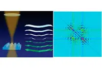
Pic: Illustration of how tiny changes in wavy images scattered from lines in a grid-like array can be reconstructed when paired with advanced optical and computational techniques. Coloring corresponds to the magnitude of the variance for specific data points
Author
Tom Austin-Morgan
Source: www.newelectronics.co.uk
 The Rice University researchers who pioneered the development of laser-induced graphene have formed it into flexible, solid-state microsupercapacitors that are claimed to charge 50 times faster than batteries, discharge more slowly than traditional capacitors and match commercial supercapacitors for both the amount of energy stored and power delivered.
The devices are manufactured by burning electrode patterns with a commercial laser into plastic sheets in room temperature air, eliminating the complex fabrication conditions that have limited the widespread application of microsupercapacitors. The researchers see a path toward cost-effective, roll-to-roll manufacturing.
"It's a pain in the neck to build microsupercapacitors now," James Tour, Professor of Chemistry, Materials Science and NanoEngineering, and Computer Science at Rice University, said. "They require a lot of lithographic steps. But these we can make in minutes: We burn the patterns, add electrolyte and cover them."
Their capacitance of 934µF/cm2 and energy density of 3.2mW/cm3 are said to rival commercial lithium thin-film batteries, with a power density two orders of magnitude higher than batteries. The researchers said the devices displayed long life and mechanical stability when repeatedly bent 10,000 times.
Prof Tour is convinced the day is coming when supercapacitors replace batteries entirely, as energy storage systems will charge in minutes rather than hours. "We're not quite there yet, but we're getting closer all the time," he said. "In the interim, they're able to supplement batteries with high power. What we have now is as good as some commercial supercapacitors. And they're just plastic."
Author
Tom Austin-Morgan
Source: www.newelectronics.co.uk