
Electronics News
Archive : 16 December 2015 год
 The Engineering and Physical Sciences Research Council (EPSRC) and Singapore’s National Research Foundation have announced a joint £2.4million research call, which will fund six joint research projects over the next three years. The projects will see UK and Singapore-based researchers collaborating to develop solutions that will enhance the resilience of systems and infrastructure to cyber attacks.
As connected global hubs and open economies, cybersecurity is of great importance to the UK and Singapore. Recognising the importance of collaboration in this area, a Memorandum of Understanding (MoU) on Cybersecurity was signed by the UK’s Cabinet Office and Singapore’s Cybersecurity Agency during Prime Minster David Cameron’s visit to Singapore in July 2015. This joint research programme implements the joint R&D collaboration element of the MoU and has been welcomed by both governments.
Minister for the Cabinet Office and Paymaster General Matt Hancock, said: “The research partnership between British and Singaporean universities will help both of our countries keep pace with the evolving cyber threat. I have no doubt that these projects will produce ground-breaking cyber security research and help protect us from threats online.”
The Singapore-UK joint grant call seeks to strengthen knowledge and capabilities in cybersecurity and foster closer collaboration in cybersecurity research between the researchers of both countries. The grant call closed in July 2015 with a total of 22 proposals received. All submitted proposals were evaluated jointly by cybersecurity experts of both countries.
The projects that will be funded under this programme are:
- The University of Oxford and the National University of Singapore will work on Security and Privacy in Smart Grid Systems: Countermeasure and Formal Verification
- The University of Kent will work with the National University of Singapore on Vulnerability Discovery using Abduction and Interpolation
- The University of Surrey and Singapore Management University will work on Computational Modelling and Automatic Non-intrusive Detection Of Human Behaviour-based Insecurity
- Imperial College and the National University of Singapore will work on Machine Learning, Robust Optimisation, and Verification: Creating Synergistic Capabilities in Cybersecurity Research
- Imperial College and Singapore University of Technology and Design will work on Security by Design for Interconnected Critical Infrastructures
- The University of Southampton and Nanyang Technological University will develop cybersecurity solutions for smart traffic control systems.
Author
Tom Austin-Morgan
Source: www.newelectronics.co.uk
 A team of engineers from Cornell University, the University of Notre Dame and the semiconductor company IQE has created gallium nitride (GaN) power diodes capable of serving as the building blocks for future GaN power switches. These switches could be used in applications spanning nearly all electronics products and electricity distribution infrastructures.
Silicon-based semiconductors are rapidly approaching their performance limits within electronics, so materials such as GaN are being explored as potential replacements that may render silicon switches obsolete.
But along with having many desirable features as a material, GaN is notorious for its defects and reliability issues. So the team has focused on devices based on GaN with record-low defect concentrations to probe GaN's performance limits for power electronics.
"Our engineering goal is to develop inexpensive, reliable, high-efficiency switches to condition electricity to replace generations-old, bulky, and inefficient technologies," said Zongyang Hu, a researcher at the School of Electrical and Computer Engineering, Cornell University. "GaN-based power devices are enabling technologies to achieve this goal."
The team examined semiconductor p-n junctions, made by joining p-type and n-type semiconductor materials, which have direct applications in solar cells, LEDs, rectifiers in circuits, and numerous variations in more complex devices such as power transistors.
To describe how much the device's current-voltage characteristics deviate from the ideal case in a defect-free semiconductor system, the team used a ‘diode ideality factor’: "an extremely sensitive indicator of the bulk defects, interface and surface defects, and resistance of the device," Hu explained.
The work by Cornell University is the first report of GaN p-n diodes with near-ideal performance in all aspects simultaneously: a unity ideality factor, avalanche breakdown voltage, and about a two-fold improvement in device figure-of-merits over previous records.
"Our results are an important step toward understanding the intrinsic properties and the true potential of GaN," Hu added.
Author
Tom Austin-Morgan
Source: www.newelectronics.co.uk
 In a move which it expects to revolutionise the low power WAN (LPWAN) market, the Weightless SIG has unveiled Weightless-P, an open standard tailored to deliver ubiquitous wide area IoT connectivity. The duplex wireless link is said to support adaptive data rates of up to 100kbit/s through a scalable network technology inspired by the mobile phone network.
While intended to operate in the sub 1GHz spectrum, those developing devices based on Weightless-P will have the option to work in licensed spectrum, using 12.5kHz narrowband technology.
Professor William Webb, CEO of the Weightless SIG, said: “Weightless-P is a turning point in LPWAN technology; no longer does the IoT community need to compromise between performance and cost when making connectivity decisions. Weightless-P is the definitive open standard for wide area IoT connectivity.”
According to the industry group, Weightless-P delivers the best compromise for the widest range of IoT applications. Along with low complexity, the open standard is said to enable long battery life, reliability, long range and robust security.
Derrick Wei, CEO of M2COMM, added: “Weightless-P is revolutionary; it will transform the LPWAN space by providing the very first clean slate open standard designed from the ground up for both public and private IoT deployments.”
Author
Graham Pitcher
Source: www.newelectronics.co.uk
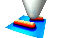 Researchers at Aalto University in Finland say they have created metallic graphene nanoribbons that are five carbon atoms wide. The results suggest the ribbons could be used as metallic interconnects in future microprocessors.
Graphene nanoribbons have been suggested as ideal wires for use in future nanoelectronics: when reduced to the atomic scale, graphene is expected to outperform copper in terms of conductance and resistance to electromigration. Until now, graphene nanoribbons have been semiconducting, which hampers their use as interconnects. But the researchers have shown that certain atomically precise graphene nanoribbon widths are nearly metallic, in accordance with earlier predictions based on theoretical calculations.
The team used scanning tunneling microscopy to probe the material’s structure and properties with atomic resolution. “We measured the properties of individual ribbons and showed that ribbons longer than 5nm exhibit metallic behaviour,” said Dr Amina Kimouche, the lead author of the paper published recently in Nature Communications.
The results are said to pave the way for using graphene in future electronic devices. The team will now work on devices combining both metallic and semiconducting graphene nanostructures. “While we are far from real applications, it is an extremely exciting concept to build useful devices from these tiny structures and to achieve graphene circuits with controlled junctions between GNRs,” said Professor Peter Liljeroth.
Author
Graham Pitcher
Source: www.newelectronics.co.uk
 IBM has opened its global headquarters for Watson Internet of Things (IoT), launching a series of new offerings, capabilities and ecosystem partners designed to extend the power of cognitive computing to the billions of connected devices, sensors and systems that comprise the IoT.These offerings will be available through the IBM Watson IoT Cloud, the company’s global platform for IoT business and developers.
Munich will serve as the global headquarters for the Watson IoT unit. The campus will bring together 1000 IBM developers, consultants, researchers and designers to drive deeper engagement with clients and partners, and will also serve as an innovation lab for data scientists, engineers and programmers building connected solutions for cognitive computing and the IoT.The centre represents IBM’s largest investment in Europe in more than two decades.
“The IoT will soon be the largest single source of data on the planet, yet almost 90% of that data is never acted upon,” said Harriet Green, general manager, Watson IoT and Education.“With its unique abilities to sense, reason and learn, Watsonopens the door for enterprises, governments and individuals to finally harness this real-time data, compare it with historical data sets and deep reservoirs of accumulated knowledge, and then find unexpected correlations that generate new insights to benefit business and society alike.”
Siemens Building Technologies is teaming with IBM to bring innovation to the digitalisation of buildings.Siemens is working to bring advanced analytics capabilities together with IBM’s IoT solutions to advance their Navigator platform for energy management and sustainability.
"By bringing asset management and analytics together with a deep technical understanding of how buildings perform, Siemens will make customers' building operations more reliable, cost-optimised and sustainable,” said Matthias Rebellius, CEO of Siemens Building Technologies."We are excited to stretch the envelope of what is possible in optimising building performance by combining the asset management and database technologies from IBM’s Watson IoT business unit with our market leading building automation domain know-how.”
Author
Tom Austin-Morgan
Source: www.newelectronics.co.uk
 Bioscience engineers from KU Leuven, Belgium, have developed an alternative method to produce Metal-organic frameworks (MOFs) in the form of very thin films, so that they can be used for high-tech applications such as microchips.
MOFs consist of a nanoporous grid of both organic molecules and metal ions. MOFs take shape as the organic molecules push the metal ions apart, so that a regular pattern of tiny holes or nanopores develops. The size of the pores can be tuned at the nanoscale level. The internal surface of an MOF, formed by these pores, varies in size from 1000 to 5000m2 per gram of material.
Professor Rob Ameloot from the KU Leuven Centre for Surface Chemistry and Catalysis, said: “Researchers are examining the use of MOFs as catalysts to accelerate chemical reactions of guest molecules in the MOF pores. Another possible application is gas storage, as the internal surface of MOFs can hold large amounts.”
So far, some applications were not considered feasible due to the production procedure for MOFs. The conventional method involves lab-scale wet chemistry, the end result of which is a powder. For integrated, nanoscale applications, the particles of that powder are too large, while a method with solutions is not pure enough. In the case of gas sensors, for instance, the MOF material has to be deposited as a thin film over the surface of the electrical circuit. That is not possible if you use the conventional production procedure.
Lead researcher, Ivo Stassen set out to find a production method other than wet chemistry. He used vapours and gases instead of liquids. “Vapour-phase deposition is already a common method to produce high-tech devices. We are the first to use this method for the production of these highly porous materials. We first deposit layers of zinc and let them react with the vapour of the organic material. The organic material permeates the zinc, the volume of the whole expands, and it is fully converted into a material with a regular structure and nanopores”, he explained.
To fine-tune the procedure, the KU Leuven researchers are collaborating with the Leuven-based research centre imec, which specialises in nanoelectronics.
“This alternative production method opens up new possibilities for MOFs in terms of applications and industries. Chemical vapour deposition is a common technique in nanofabrication. Therefore, new MOF applications can be developed relatively quickly, such as gas sensors, nanochip components, and improved batteries,” Stassen concluded.
Author
Tom Austin-Morgan
Source: www.newelectronics.co.uk
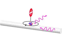 Researchers a TU Wien, in Vienna, have developed a nanoscale optical device, consisting of alkali atoms which are coupled to ultrathin glass fibres, which allows light to pass in only one direction.
Like in an electrical diode, which allows current to pass only in one direction, this glass fibre-based device transmits light only in one direction. The one-way-rule holds even if the pulse of light that passes through the fibre consists of a few photons. Such a one-way transfer of light can now be used for optical chips and may become used in optical signal processing.
“In principle, such components have been around for a long time”, said Arno Rauschenbeutel, from the Vienna Centre for Quantum Science and Technology at the Atominstitut at TU Wien. “Most optical isolators, however, are based on the Faraday Effect: A strong magnetic field is applied to a transparent material between two crossed polarisation filters. The direction of the magnetic field then determines the direction in which light is allowed to pass.”
However, devices using the Faraday Effect cannot be constructed at the nanoscale and other methods for breaking this symmetry only work at very high intensities. But in nanotechnology, an ultimate goal is to work with extremely faint light signals, which may even consist of individual photons.
Rauschenbeutel’s team chose a completely different approach: Alkali atoms were coupled to the light field of an ultrathin glass fibre. In a glass fibre, the light can propagate forwards or backwards. There is, however, another property of light which has to be taken into account: the direction of oscillation of the light wave, or polarisation.
“The polarisation rotates, like a helicopter’s rotor”, Rauschenbeutel explained. The sense of rotation depends on whether the light travels forwards or backwards. In one case, the light wave oscillates clockwise and in the other, anti-clockwise. The direction of propagation and the state of oscillation of the light wave are locked to each other.
If the alkali atoms are prepared in the right quantum state and coupled to the light in the ultrathin glass fibre, it is possible to make them react differently to the two senses of light rotation. “The light in the forward direction is not affected by the atoms. However, light which travels backwards and consequently rotates the other way around, couples to the alkali atoms and is scattered out of the glass fibre”, Rauschenbeutel continued.
This effect has been demonstrated in two different ways at TU Wien: In the first approach, about 30 atoms were placed along the glass fibre. Upon sending in light, a transmission of almost 80% was measured for one propagation direction while it was ten times less in the other direction. In the second approach, only a single rubidium atom was used. In this case, the light was temporarily stored in an optical microresonator, so that it could interact with the atom for a relatively long time. This way, similar control over the transmission could be achieved.
“When we only use one single atom, we have a much more subtle control over the process”, said Rauschenbeutel. “One can prepare the atom in a quantum superposition of the two possible states, so that it blocks the light and lets it pass at the same time.”
According to classical physics, this would be impossible, but quantum physics allows such combinations, opening the door for optical processing of quantum information.
Author
Tom Austin-Morgan
Source: www.newelectronics.co.uk
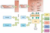 Cortus, a specialist in the development of low power, silicon efficient, 32-bit processor IP, has released the FPS26 a single precision floating point IP core. The third in a family of products based on the Cortus v2 instruction set it is aimed at embedded systems that require good floating point computational performance while also delivering small silicon area and low power dissipation.
Cortus licenses a range of low power 32-bit processor cores for intelligent connected devices. With growing numbers of controllers in solar energy and industrial control requiring floating point algorithms, many applications require floating point operations executed in hardware to achieve their performance goals. Complex matrix inversion is a challenging computation in MIMO (multiple-input and multiple-output) wireless systems due to challenges around precision, quantisation and scaling which can be mitigated by using floating point.
“For companies developing intelligent ‘things’ requiring floating point algorithms, our FPS26 core offers outstanding computational performance while efficiently using silicon area”, says Michael Chapman President & CEO of Cortus. “It fits well with the industrial internet of things and with power control applications”.
Although historically embedded software has been dominated by fixed-point operations, there are cases where values may have large dynamic ranges and floating point computation is required or is of benefit. Examples include matrix inversion in MIMO baseband processing, matrix multiplication and fast Fourier transforms (FFTs).
The FPS26 has a Harvard architecture, sixteen 32-bit registers and a 5-stage pipeline. It offers an IEEE 754 single precision hardware floating point unit, a pipelined parallel multiplier and a hardware divider. It supports the AXI4-Lite bus as well as Cortus APS peripherals. Its small size makes it suitable for cost sensitive applications.
The CPU starts at around 0.192 mm2 using a 90 nm technology. Using the Linpack benchmark FPS26 delivers 9.7 times better floating point performance than the APS25 integer core.
Up to eight co-processors can be added to an FPS26 core. The Cortus coprocessor interface allows licensees to add custom coprocessors, for example to accelerate computations in cryptography or signal processing, without knowing details of the internals of the core. Co-processor instructions can be inserted into C-code appearing as function calls.
All cores interface to Cortus’ peripherals including Ethernet 10/100 MAC, USB 2.0 Device and USB 2.0 OTG via the efficient APS bus. They also share the simple vectored interrupt structure which ensures rapid, real time interrupt response, with low software overhead.
The APS tool chain and IDE (for C and C++) is available to licensees free of charge, and can be customised and branded for final customer use. Ports of various RTOSs are available such as FreeRTOS, Micrium µC/OSII, Micrium µC/OSIII & TargetOS.
Author
Neil Tyler
Source: www.newelectronics.co.uk
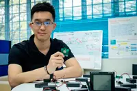 A team from Nanyang Technological University, Singapore (NTU Singapore), led by Assistant Professor Wen Yonggang from NTU’s School of Computer Engineering, has developed an algorithm that could help companies and factories cut their energy bills by as much as 10%.
The algorithm is able to analyse energy consumption by connecting to sensors in computer chips already found in equipment such as computers, servers, air conditioning systems and industrial machinery. Such computer chips are needed for a host of functions such measuring temperature, logging data traffic and monitoring the workload of computer processors.
By combining it with externally-placed sensors, such as those that monitor ambient temperature, the technology can integrate and analyse all the operational data and recommend energy-saving solutions with almost no upfront cost.
In a typical semi-conductor factory which produces computer chips and components for computers and mobile devices, the annual electricity bill can reach SGD$50million and more.
Ted Chen, co-founder and product architect of Evercomm Singapore, the company that has licensed the algorithm, said: “With NTU’s new analytic engine, such large semi-conductor factories and campuses could save up to SGD$1m a year without a need to change much of their hardware, and instead, tune their operation and time their energy usage.
“The new algorithm allows us to use the most cost-effective way to find out where we can save energy, and our performance can be guaranteed by using real-time data.”
Even without deploying external sensors, Evercomm claims it can achieve up to 5% energy savings for companies, which are facing increased regulations worldwide on their energy usage and resulting carbon footprint.
Evercomm is looking to expand its expertise into the data centre industry. It has successful deployed a pilot test at the NTU Green Datacentre, saving 5% of its monthly electricity bill.
“Our next challenge is to look into how we can deploy our energy saving analytics into apartments and housing estates,” Chen finished.
Pic: Evercomm co-founder Ted Chen holding the wireless sensor chip
Author
Tom Austin-Morgan
Source: www.newelectronics.co.uk
 STMicroelectronics has announced that it will collaborate with Semtech on its LoRa long-range wireless RF technology. ST intends to use the technology to target Internet of Things (IoT) deployments by mobile network operators (MNOs) and large-scale private networks.
ST will join the LoRa Alliance and release reference designs for LoRa technology based on its STM32 microcontrollers. ST plans to develop microcontrollers with on-chip LoRa technology that supports the LoRaWAN standardised protocol. Semtech and ST will cooperate to integrate LoRa technology into multiple platforms that target a variety of applications for several business initiatives around LoRa.
Marc Pegulu, vice president and general manager of Semtech’s Wireless, Sensing and Timing product group, said: “ST, with its strong presence in the industrial and connectivity market, reinforces that Semtech’s LoRa RF technology, LoRaWAN protocol, IP and chip-set are becoming the de-facto standards for IoT LPWANs.”
Claude Dardanne, executive vice president and general manager of the Microcontroller, Memory & Secure MCU Group, STMicroelectronics, added: “By contributing our IP and SoC design expertise, we anticipate promoting the deployment of more LPWANs worldwide, and enabling many applications with a standardised ecosystem of service providers and solutions developers.”
Author
Tom Austin-Morgan
Source: www.newelectronics.co.uk