
Electronics News
Archive : 28 December 2015 год
 Panasonic has developed a soft, flexible, and stretchable polymer resin film using its proprietary stretchable resin technology. The Company will also provide a transparent electrode material and conductive paste along with this insulating film.
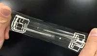
This insulating film material is claimed to stretch to 2.5 times its original length and then returns to its original shape, a feature that is said to be hard to find in conventional flexible materials. It adapts to desired manners of folding and to varying free-form surfaces, reducing existing design constraints. For example, it is said to enable the construction of soft and stretchable electronic devices that are adaptable to a variety of forms.
Using a stretchable resin as a base material, Panasonic has also developed a transparent electrode material and conductive paste that remain conductive even after repeated cycles of stretch and restore. The transparent electrode material comprises a thin conductive layer of carbon nanotubes formed on the base material of stretchable resin. The conductive paste was produced by combining the stretchable resin, used as a binder, with silver filler.
The newly developed material is claimed to be deployable in a range of applications, from wearable devices to sensors, displays, and robots.
Author
Tom Austin-Morgan
Source: www.newelectronics.co.uk
 Researchers at MIT, the University of California at Berkeley, and the University of Colorado have produced a working optoelectronic microprocessor, which computes electronically but uses light to move information. The chip was produced using only processes found in existing microchip fabrication facilities, proving that the design can be scaled up for commercial production.
Demonstrating that low power optical chips can be built with no alteration to existing semiconductor manufacturing processes should make optical communication more attractive to the computer industry. But it also makes an already daunting engineering challenge even more difficult.
“You have to use new physics and new designs to figure out how you take ingredients and process recipes that are used to make transistors, and use those to make photodetectors, light modulators, waveguides, optical filters, and optical interfaces,” explained MIT professor of electrical engineering Rajeev Ram, referring to the optical components necessary to encode data onto different wavelengths of light, transmit it across a chip, and then decode it.
The new chip marks the next step in the evolution of fibre optic communication technology by integrating into a microprocessor the photonic interconnects, or I/O, needed to communicate with other chips.
"This is a milestone. It's the first processor that can use light to communicate with the external world," said Vladimir Stojanovic, an associate professor of electrical engineering and computer sciences at the University of California, Berkeley. "No other processor has the photonic I/O in the chip."
The chip has 850 optical components and 70million transistors, which, while less than the billion-odd transistors of a typical microprocessor, is enough to demonstrate all the functionality that a commercial optical chip would require. In tests, the researchers found that the performance of their transistors was virtually indistinguishable from that of all-electronic computing devices built in the same facility.
Today’s chips cannot keep logic circuits supplied with enough data to take advantage of their ever-increasing speed. Boosting the bandwidth of the electrical connections between logic and memory would require more power, and that would raise the chips’ operating temperatures to unsustainable levels.
Optical data connections are, in principle, much more energy efficient. And unlike electrical connections, their power requirements don’t increase dramatically with distance. So optical connections could link processors that were meters rather than micrometers apart, with little loss in performance.
The researchers’ chip was manufactured by GlobalFoundries, which uses a silicon-on-insulator process, where layers of silicon are insulated by layers of glass. The researchers build their waveguides - the optical components that guide light - atop a thin layer of glass on a silicon wafer. Then they etch away the silicon beneath them. The difference in refractive index between the silicon and the glass helps contain light travelling through the waveguides.
In an optoelectronic chip light signals have to be converted to electricity. But contact with metal interferes with optical data transmission. The researchers found a way to pattern metal onto the inner ring of a donut-shaped optical component called a ring resonator. The metal doesn’t interact with light travelling around the resonator’s outer ring, but when a voltage is applied to it, it can either modify the optical properties of the resonator or register changes in a data-carrying light signal, allowing it to translate back and forth between optical and electrical signals.
On the new chip, the researchers demonstrated light detectors built from these ring resonators that are so sensitive that they could get the energy cost of transmitting a bit of information down to about a picojoule, or one-tenth of what all-electronic chips require, even over very short distances.
The authors emphasised that these adaptations all worked within the parameters of existing microprocessor manufacturing systems, and that it will not be difficult to optimise the components to further improve their chip's performance.
Author
Tom Austin-Morgan
Source: www.newelectronics.co.uk
 Carbon nanotubes are legendary in their strength - at least 30 times stronger than Kevlar by some estimates. When mixed with lightweight polymers such as plastics and epoxy resins, the tiny tubes reinforce the material, like the rebar in a block of concrete, promising lightweight and strong materials for airplanes, spaceships, cars and even sports equipment.
While such carbon nanotube-polymer nanocomposites have attracted enormous interest from the materials research community, a group of scientists now has evidence that a different nanotube, made from boron nitride, could offer even more strength per unit of weight.
Boron nitride, like carbon, can form single-atom-thick sheets that are rolled into cylinders to create nanotubes. By themselves boron nitride nanotubes are almost as strong as carbon nanotubes, but their real advantage in a composite material comes from the way they stick to the polymer.
"The weakest link in these nanocomposites is the interface between the polymer and the nanotubes," said Changhong Ke, associate professor in the mechanical engineering department at the State University of New York at Binghamton. “If you break a composite, the nanotubes left sticking out have clean surfaces, as opposed to having chunks of polymer still stuck to them. The clean break indicates that the connection between the tubes and the polymer fails.”
The researchers tested two forms of polymer: epoxy and poly(methyl methacrylate), or PMMA. They found that the epoxy-boron nitride nanotube interface was stronger than the PMMA-nanotube interface. They also found that both polymer-boron nitride nanotube binding strengths were higher than those reported for carbon nanotubes – 35% higher for the PMMA interface and approximately 20% higher for the epoxy interface.
Boron nitride nanotubes likely bind more strongly to polymers because of the way the electrons are arranged in the molecules. In carbon nanotubes, all carbon atoms have equal charges in their nucleus, so the atoms share electrons equally. In boron nitride, the nitrogen atom has more protons than the boron atom, so it hogs more of the electrons in the bond. The unequal charge distribution leads to a stronger attraction between the boron nitride and the polymer molecules. This was verified by molecular dynamics simulations performed by Dr Xianqiao Wang's group at the University of Georgia.
Boron nitride nanotubes are also said to be more stable at high temperatures than carbon nanotubes and they can better absorb neutron radiation, both advantageous properties in the extreme environment of outer space. In addition, boron nitride nanotubes are piezoelectric, which means they can generate an electric charge when stretched. This property means the material offers energy harvesting as well as sensing and actuation capabilities.
There is a drawback to boron nitride nanotubes: the cost. Currently they sell for about $1000 per gram, compared to the $10 to 20 per gram for carbon nanotubes. However, Ke is optimistic that the price will come down, noting that carbon nanotubes were similarly expensive when they were first developed.
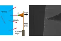
Pic: Researchers tested the force required to pluck a boron nitride nanotube (BNNT) from a polymer by welding a cantilever to the nanotube and pulling. The experimental set-up is shown in a schematic on the left and an actual image on the right.
Author
Tom Austin-Morgan
Source: www.newelectronics.co.uk
 Researchers at the UCLA Henry Samueli School of Engineering and Applied Science have identified a way to make a semiconductor laser that operates at terahertz frequencies.
Terahertz waves can be used to analyse plastics, clothing, semiconductors and works of art without damaging the materials being examined; for chemical sensing and identification; and to investigate the formation of stars and composition of planetary atmospheres.
Researchers led by Benjamin Williams, a UCLA associate professor of electrical engineering, have created the first vertical-external-cavity surface-emitting laser, or VECSEL, that operates in the terahertz range. VECSELs that use visible light have been used to generate high-powered beams, but the technique has not previously been adapted for terahertz frequencies.
To make it possible to build an external cavity laser with a high-quality beam, the UCLA researchers created a VECSEL with a ‘reflectarray metasurface mirror’. The device is made up of an array of many small antenna-coupled laser cavities such that when a terahertz wave hits the array, it doesn’t ‘see’ the cavities, but is reflected as if it were being reflected from a simple, flat mirror. Unlike a mirror however, the device amplifies the terahertz waves as well as reflecting them.
“This is the first time a metasurface and a laser have been combined,” Williams said. “The VECSEL approach provides a route to have higher output powers simultaneously with excellent beam quality in the terahertz range. The metasurface approach further allows one to engineer the beam to have the desired polarisation, shape and spectral properties.”
Creating a beam that is symmetrical and straight over large distances and changing thermal conditions is a challenge for many semiconductor lasers, but particularly for terahertz quantum cascade lasers, which usually use metal laser cavities with dimensions much smaller than the wavelength.
Luyao Xu, a graduate researcher in Williams’ lab, said, “By using this amplifying metasurface as part of the external cavity, not only can we improve the beam pattern, but we can also introduce new functionality to this laser with different cavity designs. For example, by using a freestanding wire-grid polariser, or filter, as a second mirror, we could optimise the lasers’ output power and efficiency simply by rotating the polariser.”
The researchers are working on several new designs to further advance the technology.
Author
Tom Austin-Morgan
Source: www.newelectronics.co.uk