
Electronics News
Archive : 18 January 2016 год
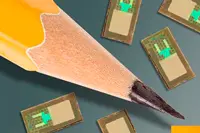 A team of neurosurgeons at Washington University School of Medicine in St.Louis and engineers at the University of Illinois has developed wireless brain sensors that monitor intracranial pressure and temperature and then are absorbed by the body, negating the need for surgery to remove them.
Such implants could be used to monitor patients with traumatic brain injuries, but the researchers believe they can build similar absorbable sensors to monitor activity in organ systems throughout the body.
"Electronic devices and their biomedical applications are advancing rapidly," said Rory Murphy, MD, a neurosurgery resident at Washington University School of Medicine. "But implants placed in the body often trigger an immune response, which can be problematic for patients. The benefit of these new devices is that they dissolve over time, so you don't have something in the body for a long time period, increasing the risk of infection, chronic inflammation and even erosion through the skin or the organ in which it's placed."
When patients with traumatic brain injuries arrive at a hospital, doctors must be able to accurately measure intracranial pressure in the brain and inside the skull because an increase in pressure can lead to further brain injury, and there is no way to reliably estimate pressure levels from brain scans or clinical features in patients.
"However, the devices commonly used today are based on technology from the 1980s," Dr Murphy explained. "They're large, they're unwieldy, and they have wires that connect to monitors in the intensive care unit. They give accurate readings, and they help, but there are ways to make them better."
The team’s devices are smaller than the tip of a pencil and are made mainly of polylactic-co-glycolic acid (PLGA) and silicone. They can transmit accurate pressure and temperature readings, as well as other information.
John Rogers, professor of materials science and engineering at the University of Illinois, explained: "With advanced materials and device designs, we demonstrated that it is possible to create electronic implants that offer high performance and clinically relevant operation in hardware that completely resorbs into the body after the relevant functions are no longer needed."
Having shown that the sensors are accurate and that they dissolve in a saline solution and then in the brains of laboratory rats, the researchers now are planning to test the technology in patients.
Author
Tom Austin-Morgan
Source: www.newelectronics.co.uk
 A research team from Japan, led by Takashi Sekiguchi of the Nano-Electronic Materials Unit, International Centre for Materials Nanoarchitectonics and Koichi Kakimoto, a professor at the Research Institute for Applied Mechanics, Kyushu University, has developed a method to grow high-quality mono silicon at low cost.
The research resulted in a casting method the researchers have called the single-seed cast method. They say it has improved the quality of crystals created compared to conventional casting methods, which could potentially lead to the development of more efficient silicon solar cells.
The current conversion efficiency of mainstream silicon-type solar cells has reached 20%; it is required in future development to increase conversion efficiency to add higher value to the cell products. However, it is said that this goal is not achievable using conventionally cast polycrystalline silicon. In addition, there is demand for the development of a silicon material to replace polycrystalline silicon and single-crystal silicon for semiconductors, as the price of dislocation-free single crystal silicon is not adequately competitive.
The researchers claim that their single-seed cast method has succeeded in growing a high-quality single-crystal silicon (mono silicon) ingot with low impurity. In this casting method, silicon is melted in a crucible, and a single crystal is grown from a small seed crystal. This method is said to be less expensive than the method to create single crystal silicon for semiconductors due to reduced raw material use and manufacturing costs.
Moreover, the conversion efficiency of a solar cell prototype created using the crystal grown by this method was as high as 18.7%. This is close to the efficiency of dislocation-free single-crystal silicon (Czochralski (Cz) silicon) wafers for semiconductors, which were evaluated concurrently and scored and efficiency of 18.9%. In future studies, the conversion efficiency of mono silicon may exceed that of Cz silicon by further reducing crystal defects and the impact of impurities.
The researchers say that their technology is compatible with, and can be integrated into existing production lines and can feasibly grow an ingot as large as 50cm3.
Author
Tom Austin-Morgan
Source: www.newelectronics.co.uk
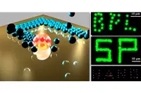 Researchers at the Cockrell School of Engineering at The University of Texas at Austin have developed a device and technique called bubble-pen lithography, which can handle nanoparticles, tiny pieces of gold, silicon and other materials used in nanomanufacturing, without damaging them. The method uses microbubbles to inscribe nanoparticles onto a surface.
Using microbubbles, the technique allows researchers to quickly, gently and precisely handle the tiny particles to more easily build tiny machines, biomedical sensors, optical computers, solar panels and other devices. This advanced control is key to harnessing the properties of the nanoparticles.
Using their bubble-pen device, the researchers focus a laser underneath a sheet of gold nanoislands to generate a hotspot that creates a microbubble out of vaporised water. The bubble attracts and captures a nanoparticle through a combination of gas pressure, thermal and surface tension, surface adhesion and convection. The laser then steers the microbubble to move the nanoparticle to a site on the surface. When the laser is turned off, the microbubble disappears, leaving the particle on the surface. If necessary, the researchers can expand or reduce the size of the microbubble by increasing or decreasing the laser beam's power.
"The ability to control a single nanoparticle and fix it to a substrate without damaging it could open up great opportunities for the creation of new materials and devices," assistant professor, Yuebing Zheng said. "The capability of arranging the particles will help to advance a class of materials, known as metamaterials, with properties and functions that do not exist in current natural materials."
According to Prof Zheng, bubble-pen lithography can leverage a design software program in the same way as a 3D printer, so it can deposit nanoparticles in real time in a pre-programmed pattern or design. The researchers were able to write the UT Austin Longhorn symbol and create a dome shape out of nanoparticle beads.
In comparison to other existing lithography methods, bubble-pen lithography has several advantages, Prof Zheng says. First, the technique can be used to test prototypes and ideas for devices and materials more quickly. Second, the technique has the potential for large-scale, low-cost manufacturing of nanomaterials and devices. Other lithography techniques require more resources and a clean room environment.
Prof Zheng hopes to advance bubble-pen lithography by developing a multiple-beam processing technique for industrial-level production of nanomaterials and nanodevices. He is also planning to develop a portable version of the technique that works like a mobile phone for use in prototyping.
Author
Tom Austin-Morgan
Source: www.newelectronics.co.uk
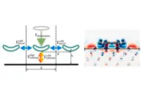 German researchers at Technische Universität München (TUM) have studied how electronic interactions govern the encounter between a molecule called porphine and copper and silver surfaces.
As electronic components continue to shrink, top-down manufacturing methods begin to approach a physical limit at the nanoscale. Rather than continue to chip away at this limit, one solution involves using the bottom-up self-assembly of molecular building blocks to build nanoscale devices.
For successful self-assembly to work the attractive and repulsive forces within molecules, between each molecule and its neighbours, and between molecules and the surface that supports them, all have to be taken into account. To better understand the self-assembly process, researchers at TUM have characterised the contributions of all interaction components, such as covalent bonding and van der Waals interactions between molecules and between molecules and a surface.
"In an ideal case, the smallest possible device has the size of a single atom or molecule," said Katharina Diller, who worked as a postdoctoral researcher at TUM.
One such example is a single-porphyrin switch, which occupies a surface area of 1nm2. The porphine molecule, which was the object of this study, is even smaller than this. Porphyrins are a group of ringed chemical compounds which include haem. Haems are most commonly recognised as components of haemoglobin, responsible for transporting oxygen and carbon dioxide in the bloodstream and chlorophyll in plants. In synthetically-derived applications, porphyrins are studied for their potential uses as sensors, light-sensitive dyes in organic solar cells, and molecular magnets.
The researchers from TUM assessed the interactions of the porphyrin molecule 2H-porphine by using density functional theory, a quantum mechanical computational modelling method used to describe the electronic properties of molecules and materials. Their simulations were performed on SuperMUC, the high-performance supercomputer at Leibniz-Rechenzentrum.
The single crystal surfaces of copper and silver metallic substrates the researchers chose for the porphyrin molecules to assemble on are widely used as substrates in surface science. This is due to the densely packed nature of the surfaces, which allow the molecules to exhibit a smooth adsorption environment. Additionally, copper and silver each react differently with porhyrins - the molecule adsorbs more strongly on copper, whereas silver does a better job of keeping the electronic structure of the molecule intact, allowing the researchers to monitor a variety of competing effects for future applications.
In their simulation, porphyrin molecules were placed on a copper or silver slab. After finding the optimal geometry in which the molecules would adsorb on the surface. To simulate different molecular coverages, the researchers altered the size of the metal slab to increase or decrease the distance between molecules. The computational setup gave them a switch to turn the energy contributions of neighbouring molecules on and off, in order to observe the interplay of the individual interactions.
The team found that the weak long-range van der Waals interactions yielded the largest contribution to the molecule-surface interaction, and showed that the often employed methods to quantify the electronic charges in the system have to be used with caution. While interactions directly between molecules are negligible, the researchers said they found indications for surface-mediated molecule-to-molecule interactions at higher molecular coverages.
"The analysis of the electronic structure and the individual interaction components allows us to better understand the self-assembly of porphine adsorbed on copper and silver, and additionally enables predictions for more complex porphyrine analogues," Diller said. "These conclusions, however, come without yet considering the effects of atomic motion at finite temperature, which we did not study in this work."
Pic: Schematic depiction of different energy terms contributing to the adsorption energy, and charge density difference of 2H-P after adsorption onto Cu(111) at 12.8 Angstrom separation
Author
Tom Austin-Morgan
Source: www.newelectronics.co.uk
 AMD has launched the Opteron A1100 processor, which it is targeting at datacentre applications. The 64bit device, manufactured on what the company calls an optimised 28nm process, features up to eight ARM Cortex-A57 cores, as well as twin 10Gbit Ethernet ports.
There are currently three members of the family planned – two of these will feature eight A57 cores, while the other will be a quad core variant. One of the eight core devices will run at 2GHz, whilst the other two parts are designed for use at 1.7GHz.
Dan Bounds, AMD’s senior director of datacentre products, described the products as the ‘first enterprise class SoCs from AMD based on ARM technology’. “They will be a turning point and a catalyst for datacentre innovation,” he contended. “The devices provide a legitimate choice when it comes to optimising workloads in datacentres and, by driving new thinking, we can help the industry innovate.”
Other features of the A1100 range include a shared 4Mbyte level 2 cache, a shared 8Mbyte level 3 cache and twin 64bit DDR3/DDR4 channels, supporting data rates of up to 1866MHz with ECC. There will also be eight PCI-Express Gen 3 lanes and 14 SATA-3 ports.
Author
Graham Pitcher
Source: www.newelectronics.co.uk
 Researchers at the University of Chicago and the US Department of Energy's Argonne National Laboratory claim to have found a way for the semiconductor industry to hit miniaturisation targets on time and without defects.
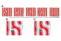
The researchers’ technique includes creating patterns on semiconductor surfaces that allow block copolymer molecules to self-assemble into specific shapes, but thinner and at much higher densities than those of the original pattern. The researchers can then use a lithography technique to create nano-trenches where conducting wire materials can be deposited.
This is a contrast to the industry practice of using homo-polymers in complex ‘photoresist’ formulations, where researchers have become unable to make the material smaller.
Before they could develop their fabrication method, however, the scientists needed to understand exactly how block copolymers self-assemble when coated onto a patterned surface - their concern being that certain constraints cause copolymer nanostructures to assemble into undesired metastable states. To reach the level to fabricate high-precision nanocircuitry, the team had to eliminate some of these metastable states.
"Molecules in these metastable states are comfortable, and they can remain in that state for extraordinarily long periods of time," explained Juan de Pablo of the University of Chicago's and Argonne's Institute for Molecular Engineering. "In order to escape such states and attain a perfect arrangement, they need to start rearranging themselves in a manner that allows the system to climb over local energy barriers, before reaching a lower energy minimum.
“What we have done in this work is predict the path these molecules must follow to find defect-free states and designed a process that delivers industry-standard nanocircuitry that can be scaled down to smaller densities without defects," he added.
De Pablo and his team used the Mira and Fusion supercomputers at the Argonne Leadership Computing Facility to generated molecular simulations of self-assembling block polymers along with sophisticated sampling algorithms to calculate where barriers to structural rearrangement would arise in the material.
After all the calculations were done, the researchers could predict the pathways of molecular rearrangement that block copolymers must take to move from a metastable to stable state. They could also experiment with temperatures, solvents and applied fields to further manipulate and decrease the barriers between these states.
"Manufacturers have long been exploring the feasibility of using block copolymer assembly to reach the small critical dimensions that are demanded by modern computing and higher data storage densities," de Pablo said. "Their biggest challenge involved evaluating defects; by following the strategies we have outlined, that challenge is greatly diminished."
The research team says it will continue their investigations with a wider class of materials, increasing the complexity of patterns and characterising materials in greater detail while also developing methods based on self-assembly for fabrication of three-dimensional structures.
Their long-term goal is to arrive at an understanding of directed self-assembly of polymeric molecules that will enable creation of wide classes of materials with exquisite control over their nanostructure and functionality for applications in energy harvesting, storage and transport.
Author
Tom Austin-Morgan
Source: www.newelectronics.co.uk
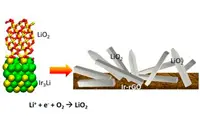 Researchers at the US Department of Energy’s Argonne National Laboratory are currently trying to find chemistries that could offer better energy possibilities. The researchers say that, of these chemistries, lithium-air could promise greater energy density.
Previous work on lithium-air batteries has shown the same phenomenon: the formation of lithium peroxide, a solid precipitate that clogged the pores of the electrode.
In a recent experiment, however, the Argonne battery scientists were able to produce stable crystallised lithium superoxide instead of lithium peroxide during battery discharging. Unlike lithium peroxide, lithium superoxide can dissociate into lithium and oxygen, leading to high efficiency and good cycle life.
"This discovery really opens a pathway for the potential development of a new kind of battery," Larry Curtiss, one of the scientists, said. "Although a lot more research is needed, the cycle life of the battery is what we were looking for."
The major advantage of a battery based on lithium superoxide, Curtiss explained, is that it theoretically allows for the creation of a lithium-air battery that consists of what chemists call a ‘closed system’. Open systems require the consistent intake of extra oxygen from the environment, while closed systems do not - making them safer and more efficient.
Khalil Amine, Curtiss’ colleague, explained: "The stabilisation of the superoxide phase could lead to developing a new closed battery system based on lithium superoxide, which has the potential of offering truly five times the energy density of lithium ion."
The scientists attributed the growth of the lithium superoxide to the spacing of iridium atoms in the electrode used in the experiment. "It looks like iridium will serve as a good template for the growth of superoxide," Curtiss said.
However, the scientists admit that they have to learn how to design catalysts to understand exactly what's involved in lithium-air batteries.
Author
Tom Austin-Morgan
Source: www.newelectronics.co.uk