
Electronics News
Archive : 2 February 2016 год
 UK semiconductor company, SmartKem has claimed to have set a world record in digital circuit performance with its tru-FLEX solution processed organic semiconductor.
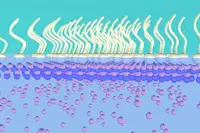
SmartKem has designed a tru-FLEX based all-organic five-stage OTFT ring oscillator using solution coating that operates with an oscillation frequency above 500kHz and stage delay of less than 200ns. This is the highest frequency reported to date for a unipolar ring oscillator fabricated using a solution processed organic semiconductor and gate dielectric. It is also expected that with further optimisation of the circuit design, oscillator frequencies above 1MHz can be attained.
This result is said to open the door to a range of application possibilities. For instance with the emergence of the IoT, one market requirement that SmartKem says has not been met is for low cost, thin, flexible and disposable RFID and NFC tags for the transmission of data from devices, sensors or objects. To achieve the necessary bit rate of 53kbits/s for a RFID or NFC device operating at the standardised frequency of 13.6MHz, a stage gate delay in the logic of less than 400ns is needed. SmartKem’s ring oscillator operates below this requirement, making it suitable as a platform technology for fully printed, low cost, flexible electronics.
A more immediate application is as a TFT backplane platform for the manufacture of conformal LCD and flexible AMOLED displays. Narrow bezels can now be achieved by the use of ‘integrated gate drivers’ fabricated on the display backplane. Whilst it was once thought that this could only be achieved using inorganic materials such as LTPS, these result shows that SmartKem’s tru-FLEX could allow the manufacture of integrated gate drivers that would not only drive 4K2K displays but, would also offer physical flexibility.
Steve Kelly, CEO and founder of SmartKem, said: “This emphasises the enabling nature of materials innovation in driving forward the potential of flexible electronics, not just for applications in smart, flexible electronics for the Internet of Things, but also the unique position it holds in enabling the growth of the flexible display industry.”
Kelly claims that the solution coated tru-FLEX TFT platform can be adopted into existing display TFT backplane production lines commonly used by manufacturers in Asia without the need for any new equipment.
Author
Tom Austin-Morgan
Source: www.newelectronics.co.uk
 A group of materials scientists from the University of Wisconsin-Madison, led by Xudong Wang, a UW-Madison professor of materials science and engineering, and postdoctoral researcher Fei Wang, has developed a technique for creating two-dimensional sheets of compounds that do not naturally form such thin materials. It is said to be the first time such a technique has been successful.
The scientists believe the tiny sheets of the semiconductor zinc oxide they're growing could have huge implications for the future of a host of electronic and biomedical devices.
Prof Wang said: "What's nice with a 2-D nanomaterial is that because it's a sheet, it's much easier for us to manipulate compared to other types of nanomaterials.”
Until now, materials scientists were limited to working with naturally occurring 2-D nanosheets. These natural 2-D structures include graphene and a limited number of other compounds.
Developing a reliable method to synthesise and manufacture 2-D nanosheets from other materials has been a goal of materials researchers and the nanotechnology industry for years.
In their technique, the UW-Madison team applied a specially formulated surfactant - a detergent-like substance - onto the surface of a liquid containing zinc ions.
Due to its chemical properties, the surfactant assembles itself into a single layer at the surface of the liquid, with negatively charged sulphate ions pointed in the direction of the liquid. Those sulphate ions draw the positively charged zinc ions from within the liquid to the surface, and within hours enough zinc ions are drawn up to form continuous zinc oxide nanosheets a few atomic layers thick.
Prof Wang first had the idea for using a surfactant to grow nanosheets during a lecture he was giving in a course on nanotechnology in 2009.
"The course includes a lecture about self-assembly of monolayers," he explained. "Under the correct conditions, a surfactant will self-assemble to form a monolayer. This is a well-known process that I teach in class. So while teaching this, I wondered why we wouldn't be able to reverse this method and use the surfactant monolayer first to grow the crystalline face."
After five years of trial and error with different surfactant solutions, the idea paid off.
The researchers have found that the 2-D zinc oxide nanosheets they've grown are able to function as semiconductor transistors called a p-type, the opposite electronic behaviour of naturally occurring zinc oxide. These nanosheets have potential for use in sensors, transducers and optical devices.
The UW-Madison team is applying its surfactant method to growing 2-D nanosheets of gold and palladium, and they say the technique holds promise for growing nanosheets from all sorts of metals that wouldn't form them naturally.
Author
Tom Austin-Morgan
Source: www.newelectronics.co.uk
 A team of engineers at NASA has been chosen to build the space agency's first ever integrated photonics communications modem. This could transform everything from telecommunications, medical imaging, and advanced manufacturing to national defence.
The modem will be tested aboard the International Space Station beginning in 2020 as part of NASA's multi-year Laser Communications Relay Demonstration (LCRD). The mobile phone-sized device incorporates optics-based functions, such as lasers, switches, and wires, onto a microchip.
Once aboard the space station, the so-called Integrated LCRD LEO (Low-Earth Orbit) User Modem and Amplifier (ILLUMA) will serve as a low-Earth orbit terminal for NASA's LCRD.
Don Cornwell, director of NASA's Advanced Communication and Navigation Division, said: “NASA has relied exclusively on radio frequency based communications since its inception in 1958. Today, with missions demanding higher data rates than ever before, the need for LCRD has become more critical.”
LCRD promises to transform the way NASA sends and receives data, video and other information. It will use lasers to encode and transmit data at rates 10 to 100 times faster than current communications equipment, requiring less mass and power.
Recent developments in nanostructures, meta-materials, and silicon technologies have expanded the range of applications for these highly integrated optical chips. Furthermore, they could be lithographically printed en masse, driving down costs.
Mike Krainak, who is leading the modem's development at NASA's Goddard Space Flight Centre, said: "The technology will simplify optical system design. It will reduce the size and power consumption of optical devices, and improve reliability."
Although the modem is expected to use some optic fibre, ILLUMA is the first step in building and demonstrating an integrated photonics circuit that ultimately will embed these functions onto a chip.
"What we want to do is provide a faster exchange of data to the scientific community," Krainak said. “The goal is to develop and demonstrate the technology and then make it available to industry and other government agencies, creating an economy of scale that will further drive down costs.”
Although integrated photonics promises to revolutionise space-based science and inter-planetary communications, its impact on terrestrial uses also is equally profound. One such use is with data centres. Integrated photonics promises to reduce the cost and size of data centres while promising faster computing power.
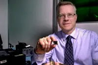
Pic: NASA laser expert Mike Krainak and his team plan to replace bulky fibre-optic receivers with an integrated-photonic circuit, whose size will be similar to the chip he is holding.
Author
Tom Austin-Morgan
Source: www.newelectronics.co.uk
 Microsoft researchers are currently testing a prototype of an underwater data centre that they say could reduce cloud latency by locating them nearer to highly populated areas and also eliminate the high-energy consumption usually attributed to data centres. Dubbed Project Natick, the data centres are said to be quickly deployable and do not require cooling.
The Natick data centres would also be connected to wind turbines or tidal energy systems to generate renewable energy for power.
“Project Natick reflects Microsoft's ongoing quest for cloud data centre solutions that provide rapid provisioning, lower costs, high responsiveness, and are more environmentally sustainable,” said Microsoft in a statement.
Microsoft's goal with Project Natick is sustainability, stating that the data centres do not create any waste products, as they're unmanned and submerged. Nor do they require any cooling solutions, with power generation for the servers provided through a turbine or a tidal energy system.
The first module was set 30 feet underwater off the coast of California for four months. The experiment was deemed such a success that engineers extended the time of the experiment and ran commercial data processing projects from Microsoft’s Azure cloud computing service. It is now being analysed at Microsoft’s Redmond campus.
Each Natick data centre deployment is estimated to last five years, after which it will be retrieved and fitted with new hardware. Microsoft says that a data centre has a lifespan of at least 20 years, after which it will be recycled.
The project itself is still in the research stages but, Microsoft claims that it is a forward-looking solution to deal with the rising energy demands at data centres.
Author
Tom Austin-Morgan
Source: www.newelectronics.co.uk