Electronics News
Archive : 25 March 2016 год
 Researchers from Empa, the Max Planck Institute in Mainz and the Technical University of Dresden claim to have produced graphene nanoribbons (GNR) with perfect zigzag edges. Electrons on these zigzag edges are said to exhibit different - and coupled - rotational directions. This is said to be a step towards creating the spintronic devices of the future.
In order to use graphene for electronic components such as field effect transistors, the material has to be ‘transformed’ into a semiconductor. The scientists achieved this by growing the nanoribbons on a metal surface from specifically designed precursor molecules. They also ‘doped’ the nanoribbons by furnishing them with impurity atoms such as nitrogen at certain points, in order to further influence the electronic properties of the GNR.
The Empa team, led by Roman Fasel, says it synthesised GNR with perfectly zigzagged edges following a specific geometry along the longitudinal axis of the ribbons. According to the scientists, this is an important step, because it can give GNR different properties via the geometry of the ribbons and especially via the structure of their edges.
The special feature of the zigzag GNR is that, along each edge, the electrons all spin in the same direction; an effect which is referred to as ferromagnetic coupling. At the same time, the so-called antiferromagnetic coupling ensures that the electrons on the other edge all spin in the opposite direction.
Thus, two independent spin-channels with opposite directions of travel arise on the band edges. Via intentionally integrated structural defects on the edges or via the provision of an electrical, magnetic or optical signal from the outside, spin barriers and spin filters can be designed that require only energy in order to be switched on and off - the precursor to a nanoscale, extremely energy efficient transistor.
According to the researchers, these properties could make GNR suitable for use in spintronic devices, which use both the charge and the spin of the electrons. This combination is prompting scientists to forecast completely new components, such as addressable magnetic data storage devices which maintain the information that has been fed in even after the power has been turned off.
Author
Tom Austin-Morgan
Source: www.newelectronics.co.uk
 New research by engineers from the Universities of Bristol and Lund, working alongside National Instruments, has demonstrated how a massive antenna system can increase spectrum efficiency by 12 times, compared with current 4G cellular technology.
Multiple antenna technology – MIMO – is used in Wi-Fi routers and 4G systems and normally involves up to four antennas. Using a flexible prototyping platform from NI based on LabVIEW system design software and PXI hardware, the Bristol configuration implements a Massive MIMO system with 128 antennas deployed at the base station.
The system used for the demonstration operates at a carrier frequency of 3.5GHz and supports simultaneous wireless connectivity to up to 12 single antenna clients. Each client shares a common 20MHz radio channel. Complex digital signal processing algorithms unravel the individual data streams in the space domain seen by the antenna array.
The demonstration achieved a bandwidth efficiency of 79.4bit/s/Hz, which equates to a throughput of 1.59Gbit/s in a 20MHz channel.
The demonstration hardware was provided to Bristol University as part of the Bristol Is Open programmable city infrastructure. Lund University, meanwhile, has a similar setup in the LuMaMi testbed, enabling researchers at both sites to work in parallel.
James Kimery, NI’s director of RF research and SDR marketing, commented: “With much discussion around 5G, NI is excited to work with top research institutions such as Bristol and Lund universities, and organisations like Bristol is Open to drive the standard forward. This Massive MIMO reference design system demonstrates the power and productivity researchers can achieve with NI tools and technologies.”
Author
Graham Pitcher
Source: www.newelectronics.co.uk
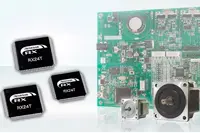
 Renesas has expanded its 32bit MCU portfolio with the addition of the RX24T group. Based on the RXv2 CPU core, the devices are said to offer enhanced performance, a decrease of 30% in development time and additional instructions that accelerate performance and energy efficiency in a range of applications.
There are six devices in the range, with 80 to 100pins and on chip flash ranging from 128 to 256kbyte. With a performance of up to 160DMIPs, the parts have dedicated analogue functions that address inverter applications, increase the arithmetic operations and expand the motor control functions of devices in the RX23T range.
The RX24T range is based on the RXv2 CPU core, with a five stage pipeline, a floating point unit and DSP functions. The company claims that, effectively, the RX24T running at 80MHz has performance levels similar to those of a comparable 100MHz device.
Board space is reduced by the RX24T integrating external circuits required by inverter control systems, such as op amps supporting simultaneous four channel amplification of three-shunt and one-shunt currents, comparators capable of overcurrent detection of amplified current, sample and hold circuits that can handle up to five channels simultaneously and DataFlash for storing log and setting files.
Author
Graham Pitcher
Source: www.newelectronics.co.uk
 With a power efficiency as high as 96%, devices from Infineon’s latest integrated power stage family can be combined with digital PWM power management controllers to provide a full multiphase voltage regulation system solution for server, storage, client and communications systems.
The devices – said to reduce power loss and to simplify design of voltage regulation solutions for multicore processors, ASICs and FPGAs and systems where efficient power management is critical – feature integration of driver technology, FET technology and package technology and are said to benefit from the combination of Infineon and International Rectifier’s capabilities.
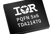
Devices in the new family come in industry standard 5 x 6mm packages and support input voltages ranging from 4.25 to 16V. Output voltage ranges from 0.25 to 5.5V and output current can be as high as 70A. Operating at up to 1.5MHz, the parts are optimised for use with 5V drive circuitry.
According to the supplier, dual edge trim dead time leads to a significant improvement in peak efficiency. Meanwhile, internal MOSFET RDS(on) current sensing, along with integrated temperature compensation, brings improved current sense accuracy versus inductor DCR sense methods. The parts also offer cycle by cycle overcurrent protection, with programmable threshold and fault flag. Additionally, there is a programmable constant current limit, while undervoltage lock out protection is said to support stable operation during system start up.
Author
Graham Pitcher
Source: www.newelectronics.co.uk
 As demand grows for thinner and lighter microelectronic devices, manufacturers can be challenged when it comes to getting power sources into the smaller space. Looking to address the issue, researchers at the University of Missouri have developed a laser writing technique that enables energy sources to be created in virtually any shape. According to the team, this approach could help smartphone manufacturers to fabricate microbatteries and micro fuel cells that are more environmentally friendly, highly designable and thin.
Assistant professor Jian Lin said: “The main goal of our research was to find an efficient and cost effective way to integrate nanostructures with micro energy storage units for applications in microelectronics. Our lab decided to test whether catalysts could be synthesised and patterned on any surface by a one step laser processing method to produce microbatteries and micro fuel cells in the shapes dictated by computer programs.”
The team adapted the DLW method to synthesise and pattern hybrid nanocatalysts – or fuel sources – into complex geometric shapes. Using computer controlled laser writing with higher heat and pressure, the scientists produced a surface that became electrically conducive and which had catalytic functionalities.
“This is the first step in manufacturing micro fuel cells and batteries that can integrate into microcircuits,” Lin claimed. “This technique has also been proven to produce microsupercapacitors. By honing the process, handheld device and smartphone manufacturers will be able to produce components in whatever shape or size they choose. Also, manufacturers will be able to choose more environmentally friendly catalysts for generating energy such as hydrogen or oxygen, which are considered cleaner fuels. The possibilities will be endless.”
Pic: Ryan Owens, University of Missouri-Columbia
Author
Graham Pitcher
Source: www.newelectronics.co.uk

