
Electronics News
Archive : 2 August 2016 год
 Tektronix has launched the TBS2000, described as a next generation basic oscilloscope with the longest record length and largest display in its class. The introduction is said to bring access to expanded capabilities, including the ability to use a range of Tektronix probes, to budget constrained design engineers.
Peter Bachmayr, technical marketing manager EMEA, said more than 800,000 units of the TDS200 have been sold to entry level and educational users since its introduction. “But challenges are greater today,” he said. “Signals are becoming more complex – PWM, for example – and don’t look like sine waves any longer. Using the TBS2000, engineers will have more measurement confidence.”
Aimed at advanced basic scope users, models are available with 70MHz or 100MHz bandwidth and with two or four channels. All feature a 9in WVGA display with 15 horizontal (time) divisions, this is said to allow users to see 50% more signal than other scopes in this category. According to Bachmayr: “While the channel colours are fixed, the cursor colours match the channel being measured.”
A 20Mpoint record length with single-knob pan and zoom provides the ability to capture long time duration signals. “Users can also trigger on runts,” said Bachmayr. “And, while there is no correlation between the time and frequency, users can see data from both domains.”
With Wi-Fi, Ethernet and USB interfaces, there is support for the Tektronix VPI probe interface – said to be for the first time in a low cost Tektronix oscilloscope – allowing access to a range of Tektronix active probes.
Author
Graham Pitcher
Source: www.newelectronics.co.uk
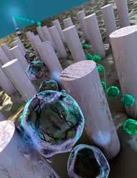 Taking advantage of the company’s experience with silicon technology, IBM scientists have developed a lab-on-a-chip device that can separate biological particles at the nanoscale. This, says the team, could enable physicians to detect diseases such as cancer before symptoms appear.
The team has already separated bioparticles of 20nm in diameter, which access to particles such as DNA, viruses and exosomes. Once separated, these particles could be analysed by physicians to reveal signs of disease before physical symptoms are seen. Until now, says the company, the smallest bioparticle that could be separated by size with on-chip technologies was about 1µm in diameter.
IBM is collaborating with the Icahn School of Medicine to develop the technology and plans to test it on prostate cancer.
Professor Dr Carlos Cordon-Cardo, chairman of the Mount Sinai Health System Department of Pathology, noted: “By bringing together Mount Sinai’s domain expertise in cancer and pathology with IBM’s systems biology experience and its latest nanoscale separation technology, the hope is to look for specific, sensitive biomarkers in exosomes that represent a new frontier to offering clues that might hold the answer to whether a person has cancer or how to treat it.”
“The ability to sort and enrich biomarkers at the nanoscale in chip-based technologies opens the door to understanding diseases such as cancer, as well as viruses like the flu or Zika,” said Gustavo Stolovitzky, IBM Research’s program director of translational systems biology and nanobiotechnology. “Our lab-on-a-chip device could offer a simple, noninvasive and affordable option to potentially detect and monitor a disease, even at its earliest stages.”
Using nanoscale deterministic lateral displacement – nano-DLD – IBM scientists Dr Joshua Smith and Dr Benjamin Wunsch led development of a technology that allows a liquid sample to be passed, in continuous flow, through a silicon chip containing an asymmetric pillar array. IBM has already scaled the chip size to 2 x 2cm, while continuing development to increase the device density to improve functionality and throughput.
According to IBM, nano-DLD uses a set of pillars to deflect larger particles while allowing smaller particles to flow through the gaps in the pillar array. The team says nano-DLD arrays can also split a mixture of different particle sizes into streams, bringing the prospect of continuous flow testing.
Author
Graham Pitcher
Source: www.newelectronics.co.uk
 North Wales based SmartKem has received patent allowance in China for its semiconductor material. The company’s truFLEX platform can be used for manufacturing flexible displays and electronics and China is seen as a key future market.
Steve Kelly, SmartKem’s CEO, said: QSuccessful collaboration is crucial in helping China to become a key stakeholder and competitor in the global OLED display industry.
“Our patent allowance places SmartKem in an excellent positon to consolidate and strengthen our existing position within the Chinese display sector with our ground-breaking semiconductor platform.”
According to the company, analysts predict that $28.7billion will be invested in OLED production across South Korea, Japan and China in the near future. Samsung is said to hold approximately 90% of the OLED market at the moment, but strong competition is beginning to emerge from China, where manufacturers are building OLED facilities, rather than LCD plants as they look to newmarkets for rigid and flexible displays.
Kelly added: “These are exciting times. This shows how far organic semiconductors have come … and emphasises the enabling nature of materials innovation and its position in enabling the growth of the flexible display industry.”
With patent allowance, the applicant needs only to pay an appropriate fee for the patent to be issued.
Author
Graham Pitcher
Source: www.newelectronics.co.uk
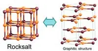 An international team of researchers has used computer simulations to find how thin a slab of salt has to be for it to break up into graphene-like layers.
Dr Pavel Sorokin, from Moscow’s Technological Institute for Superhard and Novel Carbon Materials, explained: “This work has already attracted our colleagues from Israel and Japan. If they confirm our findings experimentally, this phenomenon [of graphitisation] will provide a viable route to the synthesis of ultrathin films with potential applications in nanoelectronics.”
Previous theoretical studies suggested that films with a cubic structure and ionic bonding could spontaneously convert to a layered hexagonal graphitic structure. However, no theory had been developed that would account for this process in the case of an arbitrary cubic compound and make predictions about its conversion into graphene-like salt layers.
To study how graphitisation tendencies vary depending on the compound, the researchers examined 16 binary compounds. They all had a hexagonal, ‘graphitic’ phase that is unstable in 3D bulk but becomes the most stable structure for ultrathin 2D films. The researchers identified the relationship between the surface energy of a film and the number of layers in it for both cubic and hexagonal structures. They graphed this relationship by plotting two lines with different slopes for each of the compounds studied. Each pair of lines associated with one compound had a common point that corresponded to the critical slab thickness that makes conversion from a cubic to a hexagonal structure energetically favourable. The critical number of layers was found to be close to 11 for all sodium salts and between 19 and 27 for lithium salts.
Based on this data, the researchers established a relationship between the critical number of layers and two parameters that determine the strength of the ionic bonds in various compounds: the ionic radius and electronegativity. Higher electronegativity means more powerful attraction of electrons by the atom, a more pronounced ionic nature of the bond, a larger surface dipole, and a lower critical slab thickness.
Author
Peggy Lee
Source: www.newelectronics.co.uk