Electronics News
Archive : 18 August 2016 год
 Analog Devices has announced the acquisition of the Cyber Security Solutions (CSS) business of Sypris Electronics.
The CSS business of Sypris Electronics specialises in secure system and software technology, and delivers information security services to customers, including military and government organisations.
With this transaction, ADI says it has enhanced its aerospace and defence capabilities in the area of secure radio communications, bolsters its portfolio of system hardware and software-based cryptographic technologies, and adds a cybersecurity software and services.
ADI senior vice president, Dick Meaney, said: “We have accelerated our ability to offer our customers trust ‘from the sensor to the cloud’ through next-generation cyber-physical security solutions. The competencies and offerings of the CSS business are a great complement to our IoT solutions, as security increasingly becomes paramount to the success of IoT implementations.”
Author
Peggy Lee
Source: www.newelectronics.co.uk
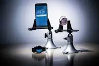
 Researchers from University of Washington (UW) have developed a way for devices as varied as brain implants, contact lenses and credit cards, to communicate with mobile devices. In one demonstration, a smartwatch transmitted a Bluetooth signal to a smart contact lens fitted with an antenna.
The team's process relies on a communication technique called backscatter, which allows devices to exchange information by reflecting existing signals. Because the technique enables Bluetooth signals to be converted into Wi-Fi transmissions, the team calls it ‘interscattering.’
"Instead of generating Wi-Fi signals on your own, our technology creates Wi-Fi by using Bluetooth transmissions from nearby mobile devices such as smartwatches," said research associate Vamsi Talla.
Interscatter communication uses the Bluetooth, Wi-Fi or ZigBee radios embedded in common mobile devices to serve as both sources and receivers for these reflected signals, potentially using 10,000 times less energy than conventional methods.
The UW team has developed an innovative way to transform Bluetooth transmissions into a ‘single tone’ signal that can be further manipulated and transformed. By backscattering that single tone signal, a contact lens could encode data -- such as health information it may be collecting -- into a standard Wi-Fi packet that could then be read by a smartphone, tablet or laptop.
"Bluetooth devices randomise data transmissions using a process called scrambling," said assistant professor Shyam Gollakota. "We figured out a way to reverse engineer this scrambling process to send out a single tone signal from Bluetooth-enabled devices such as smartphones and watches using a software app."
The challenge is that backscattering creates an unwanted mirror image copy of the signal, which consumes more bandwidth, and interferes with networks on the mirror copy Wi-Fi channel. However, the UW team developed a technique called ‘single sideband backscatter’ to eliminate the unintended by-product and freeing bandwidth.
Pic: Credit: Mark Stone/University of Washington
Author
Peggy Lee
Source: www.newelectronics.co.uk
 Researchers at ETH Zurich have developed a non-flammable battery that consists of solid chemical compounds. "Solid electrolytes do not catch fire even when heated to high temperatures or exposed to the air," explained Jennifer Rupp, professor of electrochemical materials at ETH Zurich.
One of the challenges in developing solid-state batteries is to connect the electrodes and electrolyte so that the charges can circulate between them with as little resistance as possible.
The ETH researchers have developed an improved electrode-electrolyte interface with a sandwich-like battery featuring a layer of lithium garnet, which acts as a solid electrolyte.
"During production, we made sure that the solid electrolyte layer obtained a porous surface," said researcher Jan van den Broek. The team then applied the material of the negative pole in a viscous form, allowing it to seep into the pores. Finally, the scientists tempered the battery at 100°C. "With a liquid or gel electrolyte, it is not possible to heat a battery to such high temperatures," van den Broek added.
Thanks to the trick with the pores, the researchers enlarged the contact area between the negative pole and the solid electrolyte, which means that the battery could be charged faster.
"We have, for the first time, built a lithium-ion battery with a solid lithium garnet electrolyte and a solid minus pole made of an oxide-based material. Thus, we have shown that it is possible to build whole batteries based on lithium garnet," said Prof Rupp. This will not only allow batteries to operate at higher temperatures, but also be directly placed on silicon chips.
Pic: Credit: ETH Zurich / Fabio Bergamin
Author
Peggy Lee
Source: www.newelectronics.co.uk
 Researchers from the Moscow Institute of Physics and Technology have found graphene might be suitable for manufacturing plasmonic devices capable of detecting a single molecule of explosive materials, toxic chemicals, and other organic based compounds.
Plasmon is a quasiparticle or a quantum of plasma oscillations. According to the researchers, the effects arising from the surface interactions of electromagnetic waves with plasmons could bring about a breakthrough in high-accuracy electronics and optics. One possibility opened up by plasmonic effects is the subwavelength light focusing, which increases the sensitivity of plasmonic devices to a point where they can distinguish a single molecule.
This has led to the development of a quantum model that predicts plasmonic behaviour in graphene. As a result, the scientists have described a spaser – the nanoplasmonic counterpart of the laser - whose construction involves a graphene layer.
A spaser can be described as a device similar to a laser and operating on the same basic principle. However, to produce radiation, the spaser relies on optical transitions in the gain medium, and the particles emitted are surface plasmons, as opposed to photons produced by a laser.
‘The graphene spaser could be used to design compact spectral measurement devices capable of detecting even a single molecule of a substance, which is essential for many potential applications. Such sensors could detect organic molecules based on their characteristic vibrational transitions as the light emitted/absorbed falls into the medium infrared region, which is exactly where the graphene-based spaser operates,’ said researcher Alexander Dorofeenko.
Author
Peggy Lee
Source: www.newelectronics.co.uk
![]() Cambridge Pixel has been selected by Lockheed Martin Integrated Systems to supply software modules for radar scan conversion, target tracking and radar fusion for integration into Lockheed Martin’s naval vigilance radar system.
Cambridge Pixel has been selected by Lockheed Martin Integrated Systems to supply software modules for radar scan conversion, target tracking and radar fusion for integration into Lockheed Martin’s naval vigilance radar system.
The deal is part of a £44million Royal Navy Upgrade awarded to Lockheed Martin by the UK Ministry of Defence in January 2016. As part of the contract, more than 60 Royal Navy Platforms will be fitted with the navigation radar system and SharpEye radar transceivers over the next five years.
David Johnson, CEO of Cambridge Pixel, said: “We are delighted to be working alongside Lockheed Martin’s engineers on this major upgrade of the navigation radars on the UK Royal Navy’s fleet of ships. Our technology software modules fit well with Lockheed Martin’s vision of developing a navigation radar system that meets the Royal Navy’s needs now but that also has a clear route to adding extra functionality in the future.”
The radar scan conversion module receives radar data from solid-state SharpEye radars and creates a radar image for display with underlay and overlay graphics. The radar tracking module processes the radar data to automatically acquire and track targets, and the radar fusion software combine tracks from multiple radars on ships with AIS transponder data and other sensor data into a single, integrated data source.
Pic: The Type 23 will be fitted with the navigation radar. Crown copyright.
Author
Peggy Lee
Source: www.newelectronics.co.uk
 PragmatIC has been awarded €1.6million funding under the EU’s Horizon 2020 programme (phase 2), for development of its FlexLogIC equipment.
Described as a ‘fab-in-a-box’ model, FlexLogIC is said to produce flexICs at costs between 100 and 1000 times lower than a silicon fab.
Scott White, CEO, said: “This significant grant award provides further validation of the unique and compelling nature of the FlexLogIC equipment, and its potential to drive the commercial roll-out of mass market flexible electronics."
PragmatIC’s technology platform enables the production of flexible integrated circuits that can be embedded in any surface, introducing interactivity into a range of applications from intelligent packaging of consumer goods, to wireless traceability of documents for security and identification.
Author
Peggy Lee
Source: www.newelectronics.co.uk
 A test developed at UCLA uses lab-on-a-chip technology to predict how hazardous engineered nanomaterials might be. It could also be used to identify biological biomarkers that can help scientists and doctors detect cancer and infectious diseases.
The new platform, which is called semiconductor electronic label-free assay, or SELFA, is said to cost less and be faster and more accurate than previous tests, including the enzyme-linked immunosorbent assay, or ELISA.
The SELFA chip contains a T-shaped nanowire that acts as an integrated sensor and amplifier. To analyse a sample, scientists place it on a sensor on the chip. The vertical part of the T-shaped nanowire converts the current from the molecule being analysed, and the horizontal part amplifies that signal to distinguish the molecule from others.
“By measuring biomarker concentrations in the cell culture, we showed that SELFA was 100 times more sensitive than ELISA,” Huan Meng, a UCLA assistant adjunct professor, said. “This means that not only can SELFA analyse smaller sample sizes, but also that it can minimise false-positive test results.”
Author
Peggy Lee
Source: www.newelectronics.co.uk
 UK organic semiconductor developer SmartKem has expanded its presence at the UK’s Centre for Process Innovation (CPI) with new equipment and more engineers.
The investment includes a large area slit coating machine to enable further process optimisation of truFLEX semiconductors. This allows the refinement of specific coat process protocols over large areas with nanometre control over film thickness - a critical factor in maintaining transistor uniformity and yield in the manufacture of flexible displays.
It has also upgraded its thin film transistor (TFT) test facility in Manchester – said to be UK’s only vertical science park – to enable faster validation of reliability test data for customer projects in Asia. The site has expanded to 8,000ft2 to accommodate its growing team of 30 employees.
Commenting, Steve Kelly, CEO, said: “Our investment in state-of-the-art equipment and personnel enables us to focus on developing processes and formulations that meet specific customer production line needs, speeding the technology transfer process.”
SmartKem’s organic semiconductor platform – unlike traditional inorganic materials – does not require a vacuum and is processed at room temperature using standard solution coating equipment. This is claimed to offer OEMs a high performance, unbreakable TFT platform for the production of flexible displays, sensors and logic circuits, all produced on low cost plastic substrates.
Author
Peggy Lee
Source: www.newelectronics.co.uk

