
Electronics News
Archive : 12 September 2016 год
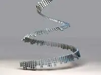
 A team from the Technical University of Munich (TUM) has discovered a double helix structure in an inorganic material. The material, called SnIP, comprising tin, iodine and phosphorus, is a semiconductor said to possess extraordinary optical and electronic properties and, unlike conventional inorganic semiconducting materials, it is highly flexible.
“These properties of SnIP are clearly attributable to the double helix,” said TUM researcher Daniela Pfister. “SnIP can be produced on a gram scale and is, unlike gallium arsenide which has similar electronic characteristics, far less toxic.”
“We have, alongside the 3D semiconducting material silicon and the 2D material phosphorene, for the first time a one dimensional material,” said TUM Professor Nilges.
Theoretical calculations by the researchers have shown that a whole range of further elements should form these kinds of inorganic double helices.
“Compared to organic solar cells, we hope to achieve higher stability from the inorganic materials. For example, SnIP remains stable up to around 500°C,” Professor Nilges explained.
Since the double helix strands of SnIP come in left and right-handed variants, materials that comprise only one of the two should supposedly display special optical characteristics. So far, however, there is no technology available for separating the two variants.
Just as with carbon nanotubes and polymer-based printing inks, SnIP double helices can be suspended in solvents like toluene. In this way, thin layers could be produced easily and cost-effectively.
The semiconducting properties of SnIP promise a wide range of application opportunities, from energy conversion in solar cells and thermoelectric elements to photocatalysts, sensors and optoelectronic elements. The fibres can be split into thinner strands only a few nanometres thick, which suggests it could also be used for nanoelectronic applications.
Author
Peggy Lee
Source: www.newelectronics.co.uk
 Evince Technology, which is developing technologies to enable the manufacture of electronics based on synthetic diamond, has closed its largest funding round to date.
According to the company, it has raised £750,240 from business angels and other private investors. The money, along with a £230,000 award from Innovate UK, will be used to strengthen parts of its technology development programme and its patent portfolio.
Evince chairman Phil Cammerman said: “This is a major milestone in the company’s development … and a significant endorsement for the company’s strategy and technology.
“Our aim is to work more closely with partners across a wide range of target applications where we believe our novel diamond technology has the potential to deliver the quantum leap in performance over silicon that the industry is urgently looking for.”
Lead investor James Morton said: “Diamond offers the potential to yield devices that are up to 100 times faster than silicon and could therefore revolutionise electronics across a broad range of industries and multi-billion dollar markets. Our investment decision was based, amongst other things, on the professionalism of the company’s approach, its passion and determination to succeed and, in particular, its rigorous development programme to deliver first prototype solid-state diamond electronic devices.”
Pic: Evince's CEO Dr Gareth Taylor with a processing tool being developed by the company
Author
Graham Pitcher
Source: www.newelectronics.co.uk
 Innovate UK is to invest up to £4million in innovative projects that help to speed the application of compound semiconductors in areas such as power electronics, RF and microwave, photonics and sensors.
According to the investment body, the competition is intended to ensure that UK businesses can respond to market opportunities in compound semiconductors. Proposals are invited that should have ‘large and scalable’ commercial potential. Projects should have total costs ranging from £50,000 to £500,000 and should last between 6 and 15 months.
All projects must involve a compound semiconductor, such as GaAs, GaN, InP, SiC and HgCdTe, and Innovate UK says it is particularly interested in projects that address topics such as thermal management, materials and techniques, hybrid combinations of silicon die with compound semiconductor die ande automated or semi automated test methodologies.
All applications must be registered by midday on 19 October and submitted before midday on 26 October.
Author
Graham Pitcher
Source: www.newelectronics.co.uk
 An international team of researchers has managed to synthesise and characterise two previously unknown silver nanoclusters of 136 and 374 silver atoms.
These diamond-shaped nanoclusters, consisting of a silver core of two to three nanometres and a protecting layer of silver atoms and organic thiol molecules, are the largest whose structure is now known to atomic precision.
Silver is a desirable material for nanocluster synthesis since it is a cheaper metal than gold and its optical properties are better controllable for applications. However, synthesis recipes that would produce silver clusters that are stable for prolonged times are not so widely known as for gold.
"From a theoretical point of view these new clusters are very interesting," said Professor Hannu Häkkinen from the Nanoscience Centre in Jyväskylä. "These clusters are already big enough that they have properties similar to silver metal, such as strong absorption of light leading to collective oscillations of the electron cloud known as plasmons, yet small enough that we can study their electronic structure in detail. Much to our surprise, the calculations showed that electrons in the organic molecular layer take part actively in the collective oscillation of the silver electrons. It seems possible to then activate these clusters by light in order to do chemistry at the ligand surface."
Author
Peggy Lee
Source: www.newelectronics.co.uk