
Electronics News
Archive : 16 October 2016 год
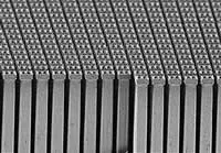
![]() University of Wisconsin-Madison engineers have revealed, in a paper published in Nature Protocols, how to create and use transparent graphene neural electrode arrays in applications in electrophysiology, fluorescent microscopy, optical coherence tomography, and optogenetics.
University of Wisconsin-Madison engineers have revealed, in a paper published in Nature Protocols, how to create and use transparent graphene neural electrode arrays in applications in electrophysiology, fluorescent microscopy, optical coherence tomography, and optogenetics.
Professor Zhenqiang Ma's group claims its see-through, implantable micro-electrode arrays for use in imaging the brain were light years beyond anything ever created.
"So many research groups started asking us for these devices that we couldn't keep up," says Prof Ma.
Although he and collaborator Prof Justin Williams patented the technology through the Wisconsin Alumni Research Foundation, they saw its potential for advancements in research.
"That little step has already resulted in an explosion of research in this field," says Williams. "We didn't want to keep this technology in our lab. We wanted to share it and expand the boundaries of its applications."
"We described how to do these things so we can start working on the next generation," Ma continues.
Now, not only are the UW-Madison researchers looking at ways to improve and build upon the technology, they also are seeking to expand its applications from neuroscience into areas such as research of stroke, epilepsy, Parkinson's disease, cardiac conditions and others.
"This paper is a gateway for other groups to explore the potential from here," Ma comments. "Our technology demonstrates one of the key in vivo applications of graphene. We expect more revolutionary research will follow in this interdisciplinary field."
Author
Peggy Lee
Source: www.newelectronics.co.uk
 Developer of energy-harvesting wireless technology, EnOcean, has announced its first modules for 2.4GHz Bluetooth Low Energy (BLE) systems. EnOcean will also now offer its energy harvesting wireless modules and white label products under the brand name ‘Dolphin’.
The first product in the EnOcean 2.4GHz BLE portfolio is the battery less PTM 215B switch module, which now comes with NFC functionality, which is said to make it easier to train and configure the switch. The PTM 215B is based on the established form factor of the PTM 21x module and can be integrated into a large number of existing switch designs. The switch is also available as a ‘white label’ end product. Applications include smart homes and modern light control.
“We’ve launched a Bluetooth switch and changed the name of EnOcean so you have Dolphin as a registered name for our harvesting products,” said UK director John Corbett. “In order to differentiate ourselves from the EnOcean sub1G, we’re now saying we’re device agnostic and have renamed the company with a brand name that covers all the radios: ZigBee, our EnOcean sub1G wireless technology and now Bluetooth Low Energy.”
EnOcean, originally a spin out of Siemens, developed a radio and radio protocol for its low power wireless kinetic harvesting switch because it was difficult to power radios and embedded processors with the 100µC the harvester needed.
EnOcean products use the energy harvesting principle, in which energy is obtained from the surroundings via energy converters to supply self-powered wireless sensor networks.
Corbett explained: “There are three core methodologies we use for energy harvesting. When converting motion into electrical energy, the switch is like a transformer. You’re basically waggling an armature inside a coil and as you move it, it will generate power and you get a switch. So the kinetic harvester is an on/off device only. It only does something when you’re making it move, such as push a button.
“We employ a Peltier device that uses the Seebeck effect for thermoelectricity; as long as you have 3° of heat difference between the front and the back of the panel, you can generate power. We also use solar energy.
Solar and thermal energies both have charge storage as well. They’ll last from three to seven days, depending on how you’ve configured them.”
Together with an efficient energy management system, the energy harvesting technology facilitates communication between maintenance-free IoT devices based on a variety of wireless standards, such as EnOcean, ZigBee and BLE.
“We’ve partnered with a company called Gooee which specialises in Bluetooth lighting. That was the kick off for the switch we have,” commented Corbett. “All the switches are compatible with each other which allows people to choose the protocol they want to use – Bluetooth, ZigBee, EnOcean – but maintain the plastics; the look and feel of the type of products they make.”
Manufacturers of BLE-based systems for the 2.4GHz band can therefore incorporate the energy harvesting technology from EnOcean into their portfolios and develop battery less, room-based wireless controllers.
Author
Peggy Lee
Source: www.newelectronics.co.uk
 A French-US team says it has improved the energy density of a rechargeable battery without increasing its size. According to the team, it achieved this by developing a 3D structure made of microtubes.
The work started from the premise that intelligent connected microsensors require miniature embedded energy sources with great energy density. For ultra thin or planar microbatteries, increased energy density means using thicker layers of materials. However, a second approach machines a silicon wafer to produce a 3D structure made of simple or double microtubes. According to the team, the 3D batteries retain a footprint of 1mm2, but have a specific area of 50mm2. These microtubes are said to be large enough to be coated with multiple layers of functional materials.
The main challenge was to deposit thin and regular layers on the complex 3D structures. Using Atomic Layer Deposition (ALD), the researchers created an insulating thin film, a current collector, a negative electrode, and a solid lithium phosphate electrolyte.
The next step will be to use ALD to develop thin films of positive electrode materials in order to create the first functional 3D prototypes.
The team comprised researchers from CNRS, Université de Lille, Université de Nantes and Argonne National Laboratory.
Author
Graham Pitcher
Source: www.newelectronics.co.uk
 In a move which is claimed to bring lower power consumption better area efficiency to memories, Kilopass has announced a Vertical Layered Thyristor (VLT) technology. Aimed at DRAM applications, VLT is said to eliminate the need for refresh and to be compatible with existing manufacturing technologies.
“Kilopass built its reputation as the leader in one-time programmable memories,” said Charlie Cheng, CEO. “As the next step on our roadmap, we examined many possible devices that would not need new materials or complex process flows and found this vertical thyristor to be very compelling.”
VLT is based on thyristor technology, electrically equivalent to a cross coupled pair of bipolar transistors that form a latch. The latch stores values and does not require refresh. Since VLT does not require refresh cycles, a VLT based DDR4 DRAM is said to reduce standby power consumption by a factor of 10 when compared to conventional DRAM at the same process node. VLT based memories can be made on current processing equipment, materials and flows, but is said to require fewer processing steps.
Kilopass expects to have test silicon by early 2017.
Author
Graham Pitcher
Source: www.newelectronics.co.uk
![]() A team of scientists is said to have set a record by creating the world's smallest transistor with a 1nm gate using a pair of novel materials: carbon nanotubes and molybdenum disulphide. The combination belongs to a class of materials called transition metal dichalcogenides, or TMDs.
A team of scientists is said to have set a record by creating the world's smallest transistor with a 1nm gate using a pair of novel materials: carbon nanotubes and molybdenum disulphide. The combination belongs to a class of materials called transition metal dichalcogenides, or TMDs.
Molybdenum disulphide, or MoS2, is an engine lubricant that scientists believe has tremendous potential in the field of electronics. Like silicon, MoS2 boasts a crystalline lattice structure. But electrons don't move as easily through MoS2 as they do through silicon.
Transistors rely on a gate to control the flow of electricity through its terminals. But because silicon allows for such a free flow of electrons, the particles barge through the doors when the gate becomes too small.
"This means we can't turn off the transistors," Sujay Desai, graduate student at Lawrence Berkeley National Laboratory, explained. "The electrons are out of control." When electrons are out of control, transistors leak energy.
With MoS2, scientists could make the gate – and the transistor – much smaller without making it susceptible to gate-crashing electrons.
"This work demonstrated the shortest transistor ever," said Professor Ali Javey from the University of California, Berkeley. "However, it's a proof of concept. We have not yet packed these transistors onto a chip, and we haven't done this billions of times over."
"Large-scale processing and manufacturing of TMD devices down to such small gate lengths will require future innovations," said Moon Kim, professor at the University of Texas.
Still, researchers are hopeful the breakthrough will translate to smaller more efficient computer chips, and ultimately, smaller, more efficient electronics.
"A cell phone with this technology built in would not have to be recharged as often," Kim said.
Author
Peggy Lee
Source: www.newelectronics.co.uk