
Electronics News
Archive : 6 January 2017 год
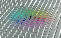 Researchers at Johannes Gutenberg University, Mainz and the Massachusetts Institute of Technology have proven that is possible to move magnetic textures, or skyrmions, backwards and forwards between different positions billions of times, which could improve memory devices.
“The spins are aligned in a way that if you walk through the hedgehog structure they twist in a spiral fashion in each direction,” explained Kai Litzius from Johannes Gutenberg University. “Because the twist is always in the same direction, the structure is called topologically protected.
“This term means that removing the skyrmion is a difficult process: it is like trying to remove the hair whorl on the back of your head. You will always have a small region of hairs pointing into a different direction - here it is outward.”
Since the skyrmions are stable, they are being considered for use in future magnetic storage devices. One of these approaches, magnetic shift register, or racetrack memory, promises low access times, high information density, and low energy consumption.
“You can imagine the ‘track’ as a small wire made of magnetic material, Litzius said. “The skyrmions would be the ‘cars’ moving along the track. Reading and writing of information on the device would be performed at fixed positions, either creating/removing a car (writing) or watching the cars pass by without interfering (reading).”
Since skyrmions can be shifted by electrical currents and feel a repulsive force from the edges of the magnetic track as well as from single defects in the wire, they can move undisturbed through the track.
“Just consider if a specific car had already passed the read unit, because it read another information first,” described Litzius. “What you do is reverse the current and shift all the skyrmions backwards until you reach the interesting slot in your chain again. This process must be able to happen millions of times to make a memory device reliable.”
“What we did in the experiment was to apply bipolar current pulses to the system. In this way, we were able to move the train of skyrmions back and forth billions of times,” Litzius concluded.
Author
Peggy Lee
Source: www.newelectronics.co.uk
 Memory chips may be able to perform tasks which were traditionally done by computer processors, according to Nanyang Technological University (NTU), Singapore in collaboration with the RWTH Aachen University and Forschungszentrum Juelich research centre.
According to the researchers, this means data could be processed where it is stored, leading to faster and thinner mobile devices and computers.
“It is like having a long conversation with someone through a tiny translator, which is a time-consuming and effort-intensive process,” NTU Assistant Professor Anupam Chattopadhyay explained. “We can now increase the capacity of the translator, so it can process data more efficiently.”
The computing circuit was built using memory chips known as Redox-based resistive switching random access memory (ReRAM). Instead of storing information, the team showed how ReRAM can be used to process data. Current devices and computers have to transfer data from the memory storage to the processor unit for computation.
The researchers believe the circuit could double the speed of current processors found in laptops and mobile devices.
The prototype ReRAM circuit processes data in four states instead of two: 0, 1, 2, or 3. Because ReRAM uses different electrical resistance to store information, it could be possible to store the data in an even higher number of states, hence speeding computing tasks beyond current limitations.
Professor Rainer Waser from RWTH Aachen University said: “ReRAM is a versatile non-volatile memory concept. These devices are energy-efficient, fast, and they can be scaled to small dimensions. Using them not only for data storage but also for computation could open a new route towards an effective use of energy in the information technology.”
Author
Peggy Lee
Source: www.newelectronics.co.uk
A plasmonic nanolaser that operates at visible light frequencies and uses dark lattice modes has been made by researchers at Aalto University, Finland. The results are said to open new prospects for on chip coherent light sources.
The laser is based on silver nanoparticles arranged in a periodic array. In contrast to conventional lasers, where the feedback of the lasing signal is provided by ordinary mirrors, the nanolaser uses radiative coupling between silver nanoparticles. The 100nm particles act as antennas.
To produce high intensity laser light, the interparticle distance was matched with the lasing wavelength so that all particles of the array radiate in unison.
According to the researchers, the challenge was that light may not exist long enough in such small dimensions to be helpful. The researchers found a way around this potential problem: they produced lasing in dark modes.
“A dark mode can be understood by considering regular antennas: a single antenna, when driven by a current, radiates strongly, whereas two antennas – if driven by opposite currents and positioned close to each other – radiate little,” explains Professor Päivi Törmä.
“A dark mode in a nanoparticle array induces similar opposite-phase currents in each nanoparticle, but now with visible light frequencies,” she continues.
“Dark modes are attractive for applications where low power consumption is needed. But without any tricks, dark mode lasing would be quite useless because the light is trapped at the nanoparticle array and cannot leave,” adds scientist Tommi Hakala.
“But we found an escape route for the light. Towards the edges of the array, the nanoparticles start to behave more like regular antennas,” concludes PhD student Heikki Rekola.
The edge nanoparticles therefore channel out the light and this nanolight is said to behave like a laser.
Author
Peggy Lee
Source: www.newelectronics.co.uk
A transparent, self-healing, stretchable, conductive material has been developed by scientists at the University of California, Riverside and the University of Colorado, Boulder. The material can be activated electrically to power artificial muscles and could be used to improve batteries, electronic devices and robots.
The researchers claim the findings represent the first time scientists have created an ionic conductor that is transparent, mechanically stretchable, and self-healing.
"Creating a material with all these properties has been a puzzle for years," said Chao Wang, an adjunct assistant professor of chemistry at Riverside.
According to the scientists, the key difficulty in self-healing is the identification of bonds that are stable and reversible under electrochemical conditions. Conventionally, self-healing polymers make use of non-covalent bonds, which are affected by electrochemical reactions that degrade the performance of the materials.
The team solved the problem by using a mechanism called ion-dipole interactions, which are forces between charged ions and polar molecules that are stable under electrochemical conditions. They attained this by combining a polar, stretchable polymer with a mobile, high-ionic-strength salt.
The low cost, rubber-like material can stretch to 50 times its original length. After being cut, it is said to completely re-attach in 24 hours at room temperature.
The material could be used to power an artificial muscle. After parts of the artificial muscle were cut into two separate pieces, the material is said to have healed without relying on external stimuli and to have returned to the same level of performance as before being cut.
The material could allow robots to self-heal after mechanical failure; extend the lifetime of lithium ion batteries used in electronics and electric cars; and improve biosensors used in the medical field and environmental monitoring.
Author
Peggy Lee
Source: www.newelectronics.co.uk
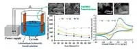 A fast and simple method to synthesise different types of copper based nanostructures has been developed by a team from the Nano-fabricated Energy Devices lab at the University of Tehran.
By applying electric fields in ammonium hydroxide based solutions, shapes such as rod, flower and cube with an average grain size of 30nm to 1μm were obtained on the copper substrate.
According to the team, the results revealed that applied electric fields considerably accelerate the formation time of nanostructures from several days to one minute, with some of the desired nanostructures being obtained in one second.
The electrochemical properties of different morphologies were compared using cyclic voltammograms, charge/discharge tests and electrochemical impedance spectroscopy. The obtained results were said to demonstrate that the structures showed high maximum areal and specific capacitance of 42mF/cm2 and 178F/g at a scan rate of 20mV/s, which the researchers claim is larger than other reports on copper hydroxide electrodes.
The structures have potential for energy devices, such as supercapacitors and lithium ion batteries.
Author
Peggy Lee
Source: www.newelectronics.co.uk