
Electronics News
Archive : 3 May 2017 год
 Using a novel controllable chemical method, Graphene Flagship researchers have created hybrid heterostructures that can be tailored to have particular electronic, magnetic and optical properties.
Stacking thin layers of graphene and related materials (GRMs) leads to heterostructure devices which can be tailored by design of the stack. The researchers use the molecular monolayers to create controllable periodic potentials on the surface of graphene.
“The mechanical superposition of different layered crystals has been proven to be a route towards the fabrication of heterostructures featuring 2D periodic potentials,” said Paolo Samorì from the University of Strasbourg.
The researchers used organic molecules that self-assembled into ordered structures on the surface of graphene.
The molecules consist of a long-chain tail and a reactive head with a small electric field caused by unequal distribution of the electrons in the head. The electric field of the heads influences the underlying graphene, while the regions covered by tails remain unaffected.
The presence of the molecules is said to lead to a periodic variation in the electric field in 1D, which can alter the behaviour of electric current in the graphene.
The properties of the molecule determine the specifics of the periodic potential. Using three different molecules, the researchers showed that the potentials can be controlled, with the size and orientation of the electric field in the head of the molecule determining the strength and type of effect in the graphene.
This new approach to device design could be extended to other GRMs, enabling more complex multilayer heterostructures with new properties. For example, in semiconductor transition metal dichalcogenides, the periodic potentials could lead to a series of nanoscale junctions with distinct optical properties.
Author
Peggy Lee
Source: www.newelectronics.co.uk
 A self-contained neural network DSP IP core from Cadence has been optimised for vision, radar/lidar and fused sensor applications. Targeted at those companies developing SoCs for the automotive, surveillance, drone and mobile/wearable markets, the Tensilica Vision C5 DSP is said to offer a capacity of 1TMAC/s, suiting it to a range of neural network computational tasks.
Designed as a dedicated neural-network-optimised DSP, the Vision C5 is said to accelerate all neural network computational layers – convolution, fully connected, pooling and normalisation. This, says Cadence, free the main vision/imaging DSP to run image enhancement applications independently, while the Vision C5 DSP runs inference tasks.
Pulin Desai, product marketing director for Cadence’s IP group, said: “The C5 is a parallel machine with special instruction set to take care of neural network processing. We looked at all the instructions and created new ones specifically for neural networks.”
Alongside the computational capacity of 1TMAC/s, the device can support 1024 8bit MACs or 512 16bit MACs and boasts a VLIW SIMD architecture with 128way 8bit SIMD or 64way 16bit SIMD.
Described as ‘flexible and future proof’, the Vision C5 supports variable kernel sizes, depths and input dimensions, as well as several coefficient compression/decompression techniques. “There will be places people want to compress coefficients and need to do on the fly decompression,” Desai added.
Occupying less than 1mm2 of silicon in a 16nm process, the core is said to perform up to six times faster than commercially available GPUs when running the AlexNet CNN performance benchmark and to run the Inception V3 CNN benchmark up to nine times faster.
Author
Graham Pitcher
Source: www.newelectronics.co.uk
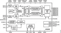 As part of a new series of high speed A/D converters, Analog Devices has launched the AD9208, said to be targeted at GHz bandwidth applications, where it meets the spectral efficiency demands of 4G/5G multi-band wireless communications base stations.
Fabricated on a 28nm CMOS process, the device is said to address multi-standard production instrumentation, as well as providing greater detection range and sensitivity for defence applications.
The dual 14bit part is optimised for wide input bandwidth, high sampling rate, high linearity and low power. Supplied in a small package with an industry standard interface, the device is said to offer designers flexibility in selecting processor platforms and signal processing partitioning.
Sampling at rates of up to 3Gsample/s, the A/D converter enables direct RF signal processing architectures and provides high oversampling. This, the company notes, simplifies front end filtering and receiver design complexity, whilst reducing system cost.
According to ADI, the AD9208 enables direct RF sampling of wideband signals at frequencies of more than 6GHz, meaning mixer stages can be eliminated. Other features include an internal clock divider and an optional RF clock output.
Supplied in a 196ball BGA measuring 12 x 12mm, the AD9208 is specified for use in temperatures ranging from -40 to 85°C.
Also introduced is the AD9172, a dual 16bit D/A converter that can sample at rates of up to 12Gsample/s. It features an eight lane, 15Gbit/s JESD204B data input port, an onchip clock multiplier and digital signal processing capabilities targeted at single- and multiband direct to RF wireless applications.
The AD9172 comes in a 144ball BGA_ED with a metal enhanced thermal lid. The package measures 10 x 10mm and the balls are on a 0.8mm pitch.
Applications for both parts include communications, test and measurement, aerospace and defence, and automotive.
Author
Graham Pitcher
Source: www.newelectronics.co.uk