
Electronics News
Archive : 8 June 2017 год
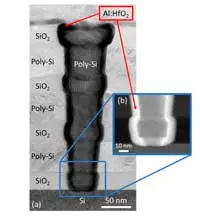 The first vertically stacked ferroelectric aluminium doped hafnium dioxide (HfO2) device for NAND applications has been demonstrated by imec.
Using a new material and a novel architecture, the Belgian nanoelectronics research centre has created a non-volatile memory concept with the potential to improve power consumption, switching speed, scalability and retention.
According to imec, ferro-electric memory has always been considered ideal, due to its very low power needs, non-volatile character and high switching speed. However, issues with the complex materials, the breakdown of the interfacial layer and bad retention characteristics have presented significant challenges. The recent discovery of a ferro-electric phase in HfO2, a well-known and less complex material, has triggered a renewed interest in this memory concept.
“With HfO2, there is now a material with which we can process ferro-electric memories that are fully CMOS compatible. This allows us to make a ferro-electric FET (FeFET) in both planar and vertical varieties,” said Jan Van Houdt, imec’s chief scientist for memory technology.
“FeFETs can be used as a technology to build memory very similar to flash memory, but with additional advantages for further scaling, simplified processing, and power consumption.
“It is, in fact, suitable for both stand-alone and embedded memories at various points in the memory hierarchy, going all the way from non-volatile DRAM to flash-like memories. It has particularly interesting characteristics for future storage-class memory, which will help overcome the current bottleneck caused by the differences in speed between fast processors and slower mass memory.”
Author
Peggy Lee
Source: www.newelectronics.co.uk
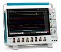 Looking to meet today’s design challenges, Tektronix has completed what it claims to be its largest development effort yet with the announcement of the 5 Series MSO mixed signal oscilloscope.
“It’s new in every regard,” said Chris Godfrey, oscilloscope business development manager for EMEA. “There’s a new ASIC with A/D converter, more channels, tighter integration and more flexibility. A lot of thought has been put into the design and how engineers will use it.”
Amongst the innovations claimed for the device is the first technology that allows either four, six or eight analogue channels, along with up to 64 digital channels. Other features include integrated protocol analysis and signal generator, a 12bit signal acquisition system and a high-definition capacitive touch display.
Designed to be flexible, capable and easy to use, the 5 Series MSO incorporates a newly designed front end amplifier said to lower noise by about 4.5dB compared to previous generation devices. It also uses a proprietary 12bit A/D converter and boasts a High Res mode that supports a vertical resolution of 16 bit.
The default input is a TekVPI+ connector that accepts all TekVPI analog probes. However, when the TLP058 Logic Probe is used, the input is converted to eight digital channels.
The scope features a 15.6in capacitive touch supporting displays of up to 1920 x 1080 pixels. Users can access controls using objects on the display, but can also drive the oscilloscope using a mouse and front-panel controls.
A removable solid state drive allows the 5 Series MSO to be used as a dedicated scope or to be based on a Windows PC platform that allows users to run other programs.
Author
Graham Pitcher
Source: www.newelectronics.co.uk
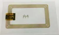 A plastic 12bit RFID tag and read-out system with screen-printed circuitry has been developed and demonstrated by Quad Industries, Agfa, imec and TNO.
The system is said to integrate, for the first time, a screen-printed antenna and a printed touch-based user interface, allowing implementation of the reader on curved surfaces. The demonstrator has been designed for security badge applications, but could find use in smart packaging, wearables and interactive games.
The access badge combines a credit-card size printed antenna and an RFID chip, integrated on a flexible plastic substrate. The RFID tag is manufactured using imec’s metal-oxide TFT technology, said to allow for inexpensive production in large quantities. The 12bit RFID developed for this demonstration contains 438 TFTs.
The read-out system contains innovative printed functionality at different levels. Firstly, an RFID read-out antenna is screen-printed on a plastic film, allowing optimal integration on flat, curved or 3D shaped reader surfaces. A fully printed touchscreen interface with numerical keypad has been added between the cover lens and the display to allow users without a badge to access the building by entering a numerical code. The printed touchscreen was printed using highly transparent screen-printed inks.
Wim Christiaens, R&D director for Quad Industries, said: “The antenna is printed at the same level as the printed touch screen, resulting in more cost effective integration of the printed antenna and the customised touch screen in the reader device.”
“This demonstration is a noteworthy example of hybrid flexible electronics, combining the advantages of plastic electronics with metal-oxide TFT technology developed by imec and TNO,” said Kris Myny, principal member of the technical staff at imec. “The technology allows for low-cost screen-printing manufacturing, is easily customisable and eco-friendly, and enables direct chip integration on various substrates, including plastics and paper. The technology promises applications in smart packaging, smart gaming and smart PCB.”
Author
Graham Pitcher
Source: www.newelectronics.co.uk
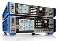 The SMA100B is the most powerful analogue signal generator on the market, Rohde & Schwarz claims, offering a frequency range of up to 20GHz.
Providing pure signals with low phase noise at all offset frequencies, a 6GHz instrument generates up to 38dBm RF output power, and a 20GHz instrument generates up to 32dBm in the microwave frequency range. Harmonics are low across the entire frequency range – above 6GHz they are lower than 70dBc at 18dBm output power. Nonharmonics are below 110dBc at an output signal of 1GHz.
"The SMA100B enables our customers to verify the true performance of their devices under test without the signal source affecting the results," says Andreas Pauly, vice president of signal generators, audio analysers and power metres.
In addition to delivering pure analogue RF signals, the generator can simultaneously provide a second, independently configurable, synchronised clock signal up to a frequency of 6GHz. As a result, users can characterise A/D converters with a single analogue signal generator.
The SMA100B is said to generate pulses with short rise and fall times and an on/off ratio of less than 90dB. Closed loop level control is available for pulse widths starting at 100ns. These characteristics make it possible to test advanced radar receivers under demanding pulse scenario conditions.
The SMA100B can provide high level signals with low, close-in phase noise (10GHz, -83dBc/Hz, 10Hz offset). The instrument's low phase noise option ensures that phase noise and wideband noise from simulated in-band or out-of-band interferers have a minimal impact on the wanted signal.
The high output power option enables the SMA100B to provide up to 38dBm of output power, eliminating the need for external amplifiers in automated test environments.
Wear-free electronic step attenuators are integrated. The SMA100B is designed for the RF semiconductor, wireless communications and aerospace and defence industries.
Author
Peggy Lee
Source: www.newelectronics.co.uk
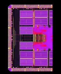 An ultra-low power IoT reference platform developed by sureCore and targeted at next generation wearable consumer and medical applications, has been taken to tape out by semiconductor IP developer EnSilica.
The IoT reference platform, which incorporates derivations of sureCore’s EverOn and PowerMiser SRAM IP product lines, has been targeted at TSMC’s 40nm Ultra Low Power process technology.
“EnSilica was a natural choice for the implementation of our IoT reference platform,” said Eric Gunn, COO of sureCore. “With a demonstrable understanding of how near threshold design can meet customer expectations for battery powered applications, EnSilica’s technical appreciation of our technology, as well as a deep understanding of TSMC’s processes, has ensured a painless route to tape-out.”
“We are pleased to extend our relationship with sureCore on the implementation of its IoT reference platform,” said Ian Lankshear, EnSilica’s CEO. “Its EverOn and PowerMiser SRAM IPs are proving a game-changer when it comes to providing SoC developers with ultra-low power, area-efficient memories and its IoT reference platform looks set to make the same impact on the next generation of wearable consumer and medical applications.”
PowerMiser is single port synchronous low power SRAM IP said to consume less than 50% of the dynamic power of industry standard SRAMS, well as a 20% static power reduction. EverOn is single port synchronous ultra low voltage SRAM IP that operates at voltages as low as 0.6V.
Author
Graham Pitcher
Source: www.newelectronics.co.uk