
Electronics News
Archive : 4 September 2017 год
 The UK government has announced six areas in the UK that will shortly be trying out broadband technology that provides data at speeds approaching one gigabit per second (gbps).
The pilots for the "full-fibre" network technology will be run in Aberdeenshire, West Sussex, Coventry and Warwickshire, Bristol, West Yorkshire and Greater Manchester.
The government said that it will spend about £10m getting the pilots up and running.
Full fibre involves taking high speed cables directly to buildings and doesn’t rely on older and slower copper for the final link, as tends to be the case with most existing fibre services in the UK.
Fast-fibre optic cables that run directly to homes or offices tend to provide a more stable, efficient and reliable connection than the hybrid systems which use copper and fibre and can support speeds up to 1Gbps.
At present, figures suggest that just 2 percent of buildings in the UK have access to full fibre networks and the government has said that it hopes these projects will help to boost the availability and take-up of the technology.
However, analysts have suggested that as full-fibre broadband gigabit-capable cables are expected to be shared between many different premises, it could mean that the actual data download speeds available to users may prove to be significantly below the theoretical maximum.
The funding for the gigabit-speed broadband pilots comes from a £200m fund announced in the budget earlier this year.
Author
Neil Tyler
Source: www.newelectronics.co.uk
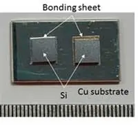 A silver micron-particle sintering joining technology has been developed by scientists at The Institute of Scientific and Industrial Research, Osaka University.
The research, conducted as part of the Advanced Low CArbon Technology Research and Development Program (ALCA) of the Japan Science and Technology Agency (JST), has developed a low-temperature pressureless die bonding, which can be used for all types of electrodes, including Cu and Au, as well as silver coating and will allow low-cost, reliable heat-resistant mounting technology for die attach and for printed wiring without changing conventional cheap electrode structures. Researchers suggest it could prove suitable for next-generation power semiconductors, such as GaN.
According to the team, led by Professor Suganuma, the new silver micron-particle sintering joining technology has enabled low-temperature and pressureless die bonding in an ambient environment at a low cost. Crucially, the technology has been able to show high reliability at high temperatures over 250°C and is proving suitable for next-generation main power semiconductor die bonding technology.
The team clarified the nano-level bonding mechanism last year, but the material of electrodes was limited to silver (Ag), because the key to that technology was based on interactions between Ag and oxygen (O).
Nickel/gold (Ni/Au) or copper (Cu) are used for electrodes for silicon (Si), silicon carbide (SiC) and gallium nitride (GaN) semiconductors as well as direct bonded copper (DBC) substrates. So, bonding to Ni/Au or Cu electrodes is in high demand, as a result the film bonding will expand the scope of its application significantly.
To solve these electrode-related challenges this group, in joint research with the Daicel Corporation, has developed a solvent that can promote interfacial activation of Ag, achieving pressureless sintering technology of joining various electrodes even at 200°C, lower than that of conventional technology. With this new type of solvent (paste), a low electrical resistivity of 4×10⁻⁶Ωcm, about two times of that of Ag, has been achieved, which can only be obtained with this new silver paste.
In conventional power semiconductor fabrication processes, films (or sheets) are often used instead of paste as a die attach material. This technology activates the surface of an Ag film by grinding it, forming hillocks on the surface of the Ag film at temperatures ranging from 200 to 250°C.
According to researchers this will enable not only high performance die bonding of next-generation power semiconductors like SiC and GaN, but also wiring according to surface roughness of a die with lower noise, by no load and low temperatures process. This will help achieve the reduction of energy loss during power conversion, which is characteristic of SiC and GaN power semiconductors.
Author
Neil Tyler
Source: www.newelectronics.co.uk
 Scientists at the University of Sussex have developed a new algorithm that will enable smartwatches to detect and record an individual’s movements, without being told beforehand what to look for.
At present while smartwatches are able to recognise a limited number of particular activities, in order to do so they have to be programmed in advance.
The new algorithm has been designed to enable the smartwatch to discover activities as they happen and can even track sedentary activities.
Commenting Dr Hristijan Gjoreski of the University of Sussex said: "Current activity-recognition systems usually fail because they are limited to recognising a predefined set of activities.” According to Dr Gjoreski this new machine-learning approach, “detects new human activities as they happen in real time, and outperforms competing approaches."
"Traditional models ' cluster' together bursts of activity to estimate what a person has been doing, and for how long," he explained.
This approach will take continuous steps and cluster them into a walk, but doesn't account for pauses or interruptions in the activity.
The new algorithm has been designed to track ongoing activity and it is able to play much closer attention to transitioning i.e. stops and starts, as well as the activity itself. For example, it will take into account short pauses and will assume that the walk will continue, holding the data while it waits.
Dr Daniel Roggen, head of the Sensor Research Technology Group at the University of Sussex, added: "Future smartwatches will be able to better analyse and understand our activities by automatically discovering when we engage in some new type of activity. This new method for activity discovery paints a far richer, more accurate, picture of daily life.
"As well as for fitness and lifestyle trackers, this can be used in healthcare scenarios and in fields such as consumer behaviour research."
Author
Neil Tyler
Source: www.newelectronics.co.uk
 A way to stop frequency fluctuation in buck converters has been found by a research team of scientists from Golestan University in Iran, US Concordia University, and Delft University of Technology in the Netherlands.
Buck converters, or step down converters, put out less power than they receive, and the tracking signals in the output can get stuck. This results in a small but harmful frequency fluctuation, or 'chatter', which is said to lead to worn hardware, temperature changes in the circuits, and to make the system difficult to accurately control.
"In order to suppress the chattering, a high order sliding mode control technique was previously proposed, and was established as the most successful chattering avoidance method," said Delft University Professor Hassan HosseinNia.
The purpose of the sliding mode control for the buck converter is to control the output voltage. The technique is said to sample the system, creating a representative sample of the system's typical behaviour.
However, according to the researchers, the control method becomes less reliable and robust if other unknown variables come into play. Since the output is known, the researchers need to control the other variables to meet the desired output.
To eliminate the chatter and better control the system, the scientists designed what they call a second order sliding mode controller via twisting algorithm.
"The adaptive sliding mode control method for controlling the buck converter voltage leads to a more effective performance against disturbances and system uncertainties than the sliding mode control method; the only difference is that in this method the parameter in the sliding line is not constant," HosseinNia explained.
By allowing flexibility in the sliding line parameter, the researchers claim they can clear the chatter while retaining robustness of the system at the output.
Author
Peggy Lee
Source: www.newelectronics.co.uk
 A device being developed by Washington State University physicists could turn the heat generated by an array of electronics into a usable fuel source.
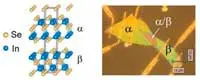
According to the scientists, the device is a multicomponent, multilayered composite van der Waals Schottky diode. They claim it converts heat into electricity up to three times more efficiently than silicon and that it could eventually provide an extra source of power for applications ranging from smart phones to automobiles.
"The ability of our diode to convert heat into electricity is very large compared to other bulk materials currently used in electronics," said associate professor Yi Gu.
"In the future, one layer could be attached to something hot like a car exhaust or a computer motor and another to a surface at room temperature. The diode would then use the heat differential between the two surfaces to create an electric current that could be stored in a battery and used when needed."
Unlike conventional Schottky diodes, the new diode is made from a multilayer of microscopic, crystalline indium selenide. The researchers used a heating process to modify one layer of the indium selenide to act as a metal and another layer to act as a semiconductor.
The diode is said to have no impurities or defects at the interface where the metal and semiconductor materials are joined together, which according to the scientists enables electricity to travel through the multilayered device with almost 100% efficiency.
"When you attach a metal to a semiconductor material like silicon to form a Schottky diode, there are always some defects that form at the interface," said researcher McCluskey.
"These imperfections trap electrons, impeding the flow of electricity. This diode is unique in that its surface does not appear to have any of these defects."
Author
Peggy Lee
Source: www.newelectronics.co.uk