
Electronics News
Archive : 7 October 2017 год
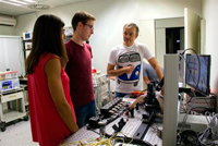 A photonic integrated chip developed by researchers from the Institute of Telecommunications and Multimedia Applications (iTEAM) at the Universitat Politècnica de València and the Optoelectronics Research Centre at the University of Southampton is said to behave similarly to a microprocessor. According to the team, just like the hardware in an MPU can perform software defined operations, its chip can perform multiple functions using a single common architecture.
“By programming the internal connections of a single chip architecture, we can configure the chip to perform different functions,” said José Capmany, iTEAM researcher and coordinator of the work.
The chip’s architecture features a honeycomb waveguide mesh implemented by properly cascading tunable light couplers developed by iTEAM researcher Daniel Pérez. An independent basic coupler configuration allows flexible interconnection schemes to be defined, as well as different optical signal processing circuits.
“The main advantage of this approach is that the physical hardware architecture is manufactured independently from the targeted functionality to be performed, which reduces the price of design, fabrication and testing iterations,” said Ivana Gasulla, who is supervising Pérez’ research.
Once fully designed and tested, the chip should enable more than 100 photonic signal processing circuits to be configured. So far, the team has demonstrated around 30 configurations. “The approach represents a paradigm shift in the field of integrated photonics; from application specific photonic integrated circuits to generic purpose and programmable devices, in the same way as [electronics] in the 1980s,” said Capmany.
A range of applications is envisaged, including mobile communications, quantum computing, distributed sensors and the IoT.
Author
Graham Pitcher
Source: www.newelectronics.co.uk
 Belgian nanotechnology research centre imec has developed a pressure sensor based on micro-optomechanical systems (MOMS) technology. The device is said to exhibit excellent measurement precision over a large pressure range while being compact, resistant to EMI. Applications are expected to include high-quality sensing, particularly in the medical and life sciences sectors.
“Our advanced sensor could be used in a variety of (biomedical) applications, such as intracranial pressure or intravascular blood pressure monitoring, where high-quality remote sensing is required. The sensor has also proven its biocompatibility and can be used in combination with MRI technology as there are no metal parts,” said Xavier Rottenberg, principal member of imec's technical staff.
MEMS-based pressure sensors are said to be popular due to their good performance and small size. Optical fibre sensors, meanwhile, are suitable for use in harsh environments, but are less integrated and more complex and expensive.
Imec’s MOMS-based device is said to combine the best of both worlds, as evidenced by its high precision. Tests have shown root mean square precision of less than 1Pa across a range that could reach 100kPa.
Author
Graham Pitcher
Source: www.newelectronics.co.uk
 Design house, Plextek RFI, has announced that it has developed a multi-chip module (MCM) to cover the recently-designated European ‘Pioneer Band’ for millimetre-wave (mmWave) 5G around 26GHz.
The development of the Front-End Module (FEM) was carried out in collaboration with Filtronic Broadband.
“The band 24.25 to 27.5GHz was designated at the end of last year by the EU Radio Spectrum Policy Group (RSPG) as the preferred band, or ‘Pioneer Band’, for mmWave 5G,” explains Liam Devlin, CEO of Plextek RFI. “We welcome the opening up of this spectrum band for 5G, but we identified early on that there was a lack of components available at this frequency, and that led us to define this joint FEM development project.”
The FEM comprises a GaAs low-noise amplifier (LNA), power amplifier (PA) and transmit/receive switch housed in a custom laminate surface-mount (SMT) package measuring 10mm x 10mm. The receive path gain is 20dB across the full band, with a noise figure of 3.5dB. Transmit path gain is 19dB, and the output referred third order intermodulation (IP3) is +36dBm. Low-loss RF filtering has been integrated into the package structure, with a band-pass filter after the LNA and a harmonic rejection filter after the PA. Insertion loss figures are 0.7dB for the band-pass filter and 0.2dB for the harmonic rejection filter.
“This development has demonstrated that we can overcome the manufacturing challenges of integrating filters along with multiple die into an SMT package,” said Mike Weaver, managing director of Filtronic Broadband. “This is not easy at mmWave frequencies, and will give us a crucial head start towards eventual production when the market demand for 5G components at 26GHz begins to ramp up.”
Author
Neil Tyler
Source: www.newelectronics.co.uk
 Some 66% of thermal engineers must wait at least a day for their thermal simulations to solve. That’s according to the new State of Thermal report from 6SigmaET, which asked 170 thermal engineers in the electronics industry – including users of nine of the top thermal simulation suites - to share their views on thermal simulation.
Thermal simulations of electronics are being modelled in ever increasing detail requiring specialist software and powerful hardware. While 66% of thermal engineers must spend a day or more waiting for their equations to solve, 32% can complete this step in under an hour suggesting a drastic difference in the capabilities of the thermal simulation packages currently on the market.
According to 6SigmaET’s research there are a number of other bottlenecks within the traditional thermal simulation process. According to 6SigmaET 39% of thermal engineers must spend over an hour simply importing their CAD models from a design suite into their current simulation platform. 51% also consider the initial model creation stage to be too slow.
Despite these concerns however, 60% of thermal engineers have not switched simulation provider for over 3 years, while almost half have never switched.
Commenting on these findings, Tom Gregory, Product Manager at 6SigmaET said, “Given the advancements made in thermal engineering over the last ten years, it’s concerning to see so many engineers still relying on outdated processes and technology to complete their designs. Through advancements such as cloud-solving, there is no reason why engineers should be spending days solving their simulations.
“Our research surveyed users of nine of the world’s leading thermal simulation packages. This analysis highlights significant loyalty, with many engineers preferring to maintain a slow or unreliable system that they know, rather than switch to a more modern – yet less familiar – tool. To address this, we believe that many of today’s simulation providers must look to simplify their suites, increasingly automating processes to cut down build times, speed up solving and ultimately shorten the average time-to-market for designs. By incorporating the latest cloud-solving technology, a familiar user interface designed to mimic traditional business software packages, an unstructured-grid solver and automated processes, the latest version of 6sigmaET overcomes all of these issues.”
To download a copy of 6SigmaET’s State of Thermal report visit https://www.6sigmaet.info/whyswitch
Author
Neil Tyler
Source: www.newelectronics.co.uk