
Electronics News
Archive : 22 November 2017 год
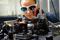 Physicists at Bielefeld University have found a way to use the heat from electronic devices to create energy, applying the heat to generate magnetic signals known as ‘spin currents’.
According to researchers it could be possible in the future to use these signals to replace some of the electrical current currently used in electronic components.
In a new study, physicists from the University of Greifswald, Gießen University, and the Leibniz Institute for Solid State and Materials Research in Dresden tested which materials generated this spin current most effectively from heat. Their findings have been published in the research journal ‘Nature Communications’.
The Bielefeld physicists are working on the basic principles for making data processing more effective and energy-efficient in the young field of ‘spin caloritronics’ and the study determines the strength of the spin current for various combinations of thin films.
A spin current is produced by differences in temperature between two ends of an electronic component. These components are extremely small and only one millionth of a millimetre thick. Because they are composed of magnetic materials such as iron, cobalt, or nickel, they are called magnetic nanostructures.
The physicists take two such nanofilms and place a layer of metal oxide between them usually only a few atoms thick. One of the external films is then heated and then electrons with a specific spin orientation then pass through the metal oxide. This produces the spin current.
The teams led by Dr. Alexander Böhnke and Dr. Torsten Hübner have tested different combinations of ultra-thin films. ‘Depending on which material we used, the strength of the spin current varied markedly,’ says Böhnke. ‘That is because of the electronic structure of the materials we used.’
According to the researchers, magnetic nanostructures with special combinations made up of cobalt, iron, silicon, and aluminium were particularly productive.
The study is one of a number of projects in the ‘Spin Caloric Transport’ (SpinCaT) Priority Programme of the German Research Foundation (DFG).
Author
Neil Tyler
Source: www.newelectronics.co.uk
 Work by researchers from Princeton University, the Georgia Institute of Technology and Humboldt University in Berlin is pointing the way to possibly more widespread use of organic electronics.
Their research, which was recently published in Nature Materials, focuses on organic semiconductors, a class of materials for seen as being used in emerging technologies such as flexible electronics, solar energy conversion, and high-quality colour displays.
In the short term, the advance could help with organic light-emitting diodes that operate at high energy to emit colours such as green and blue.
"Organic semiconductors are ideal materials for the fabrication of mechanically flexible devices with energy-saving low temperature processes," said Xin Lin, a doctoral student and a member of the Princeton research team. "One of their major disadvantages has been their relatively poor electrical conductivity, which leads to inefficient devices with a shorter operating lifetime than required for commercial applications."
In the doping process used to make semiconductors their chemical makeup is modified by adding a small amount of chemicals or impurities. By carefully choosing the type and amount of dopant, researchers are able to alter the electronic structure and electrical behaviour of the semiconductor in a number of ways.
The researchers have developed an approach that greatly increases the conductivity of organic semiconductors, which are formed of carbon-based molecules rather than silicon atoms. The dopant, a ruthenium-containing compound, is a reducing agent, which means it adds electrons to the organic semiconductor as part of the doping process. Their addition is the key to increasing the semiconductor's conductivity.
The compound belongs to a newly-introduced class of dopants called dimeric organometallic dopants. Unlike many other reducing agents, these dopants are stable when exposed to air but still work as strong electron donors both in solution and solid state.
Seth Marder and Steve Barlow from Georgia Tech, who led the development of the new dopant, called the ruthenium compound a "hyper-reducing dopant." They said it is unusual, not only its combination of electron donation strength and air stability, but in its ability to work with a class of organic semiconductors that have previously been very difficult to dope. In studies conducted at Princeton, the researchers found that the new dopant increased the conductivity of these semiconductors about a million times.
The ruthenium compound is a dimer, which means it consists of two identical molecules, or monomers, connected by a chemical bond. As is, the compound is relatively stable and, when added to these difficult-to-dope semiconductors, it does not react and remains in its equilibrium state. That posed a problem because to increase the conductivity of the organic semiconductor, the ruthenium dimer needs to split and release its two identical monomers.
The researchers looked for different ways to break up the ruthenium dimer and activate the doping, eventually they added energy by irradiating with ultraviolet light, which effectively excited the molecules in the semiconductor and initiated the reaction. Under exposure to the light, the dimers split into monomers, and the conductivity rose.
"Once the light is turned off, one might expect the reverse reaction to occur" and the increased conductivity to disappear, Marder saidl. "However, this is not the case."
The researchers found that the ruthenium monomers remained isolated in the semiconductor even though thermodynamics should return the molecules to their original configuration as dimers.
The team’s hypothesis is that the monomers are scattered in the semiconductor in such a way that it is very difficult for them to return to their original configuration and re-form the ruthenium dimer. They are, according to the team “kinetically trapped."
The researchers also discovered that doping was continuously re-activated by the light produced by the device. The light activates the system more, which leads to more light production and more activation until the system is fully activated, Marder said. "This alone is a novel and surprising observation."
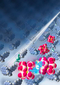
Pic: Researchers used ultraviolet light to excite molecules in a semiconductor, triggering reactions that split up and activated a dopant.
Author
Neil Tyler
Source: www.newelectronics.co.uk
 A research team at the National University of Singapore (NUS) has developed a soft, flexible and stretchable microfibre sensor for real-time healthcare monitoring and diagnosis.
Highly sensitive and ultra-thin with a diameter of a strand of human hair, the sensor has been designed to be both simple and cost-effective to mass produce.
While wearable and flexible technology has gained significant interest in recent years, current devices have various limitations – for instance, they may not fit well on the skin or are uncomfortable to wear.
According to Professor Lim Chwee Teck from the Department of Biomedical Engineering at NUS Faculty of Engineering, who is the leader of the research team, “Our novel microfibre sensor can hardly be felt on the skin and conforms extremely well to skin curvatures. Despite being soft and tiny, the sensor is highly sensitive and it also has excellent electrical conductivity and mechanical deformability. We have applied the sensor for real-time monitoring of pulse waveform and bandage pressure. The results are very promising,”
The smart microfibre sensor developed by the NUS Engineering team comprises a liquid metallic alloy, which serves as the sensing element, encapsulated within a soft silicone microtube. The sensor measures an individual’s pulse waveform in real-time, and the information can be used to determine one’s heart rate, blood pressure and stiffness in blood vessels.
“Currently, doctors will monitor vital signs like heart rate and blood pressure when patients visit clinics. This requires multiple equipment such as heart rate and blood pressure monitors. As our sensor functions like a conductive thread, it can be easily woven into a glove which can be worn by doctors to track vital signs of patients in real-time. This approach offers convenience and saves time for healthcare workers, while patients can enjoy greater comfort,” added Prof Lim.
“Our microfibre sensor is highly versatile, and could potentially be used for a wide range of applications, including healthcare monitoring, smart medical prosthetic devices and artificial skins. Designed to be durable and washable, it is highly attractive for promising applications in the emerging field of wearable electronics,” said Prof Lim.
Researchers are currently refining the sensor design and reducing the size of its accessories to improve the user-friendliness of the device.
Pic: Professor Lim Chwee Teck
Author
Neil Tyler
Source: www.newelectronics.co.uk
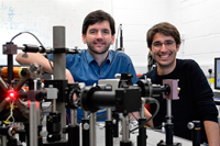 Researchers at the University of Cambridge, working with a team from TU Eindhoven, have used 3D nanoprinting to create a nanoscale magnetic circuit which is said to be capable of moving information in three dimensions. The team claims this could lead to an ‘important increase’ in storage and processing capacities.
“We have demonstrated a new way to fabricate and use a magnetic device which, in a nanometric scale, can controllably move information along the three dimensions of space,” said Amalio Fernández-Pacheco from the Cavendish Laboratory in Cambridge.
Nano-magnets in an electron microscope, along with a gas injector, were used to 3D print a suspended scaffold on a 2D silicon substrate. After 3D nano-printing, magnetic material was deposited over the ensemble. By combining precise fabrication protocol with an tailor-made laser system, the researchers have demonstrated the detection of structures which are almost completely suspended and have widths of 300nm.
“Not only have we demonstrated a big leap in nanofabrication capacities, but, importantly, we have also developed a system which allows us to look at these tiny devices in a relatively simple way,” noted lead researcher Dédalo Sanz-Hernández. “The information within the device can be read using a single laser in dark-field configuration.”
“Projects such as this open the path to the development of a completely new generation of magnetic devices that can store move and process information in a very efficient way by exploiting the three dimensions of space,” Fernández-Pacheco concluded.
Amalio Fernández-Pacheco, (left) and Dédalo Sanz-Hernández. Pic: Dédalo Sanz-Hernández
Author
Graham Pitcher
Source: www.newelectronics.co.uk
 Imec and Panasonic have announced that they have developed a solid nanocomposite electrolyte for next-generation batteries with a lithium ion conductivity several times greater than its liquid equivalent.
The ion conductivity already reaches several mS/cm at room temperature and imec and Panasonic have set a goal to develop innovative solid nanocomposite electrolyte materials towards 100mS/cm in the next few years, which would make them suitable for fast-charging high-energy cells for use in vehicles and electronics.
Li-ion batteries are the predominant type of storage in the portable electronics and electrical vehicle markets and are poised to take an important role in the future energy grid, where they have the capacity to store energy from sustainable energy sources.
Li-ion batteries, however, still require considerable innovation in order to achieve ultra-fast-charging high-energy cells and to accelerate this, imec has set up a partner programme concentrating on solid-state batteries.
“One of the unique benefits of imec is that we can leverage our state-of-the-art semiconductor knowledge to solve challenges in other research domains such as smart energy,” explained Philippe Vereecken, principal member of technical staff and program manager at imec. “This is what we have done to develop a novel solid nanocomposite electrolyte (SCE) which is deposited from solution. The wet chemical preparation route allows the solid-state electrolyte to be casted into powder electrodes, where it solidifies while remaining mechanically pliable. This paves the way to batteries in flexible form factors.”
According to Vereecken, Imec’s and Panasonic’s SCE is a mesoporous silica monolith functionalised with specific surface chemistry and ionic salts and has achieved Li-ion conductivities of 3 to 10mS/cm at room temperature, “which is exceptionally high for solid electrolytes that are applied via wet chemical coating.
“Moreover, using a new electrolyte technology, we have demonstrated rechargeable solid-state Li-ion batteries with lithium titanate (Li4Ti5O12) as negative electrode and lithium iron phosphate (LiFePO4) as positive electrode.”
Author
Neil Tyler
Source: www.newelectronics.co.uk