
 Researchers at the University of Illinois at Urbana-Champaign have developed a process for geometrically transforming 2D micro/nanostructures into extended 3D layouts.
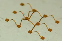
"Conventional 3D printing technologies are fantastic," said Professor John Rogers, "but none offers the ability to build microstructures that embed high performance semiconductors. We have presented a remarkably simple route to 3D that starts with planar precursor structures formed in nearly any type of material, including the most advanced ones used in photonics and electronics.
"A stretched, soft substrate imparts forces at precisely defined locations across such a structure to initiate controlled buckling processes that induce rapid, large-area extension into the third dimension. The result transforms these planar materials into well-defined, 3D frameworks with broad geometric diversity."
Initial demonstrations are said to include experimental and theoretical studies of more than 40 geometries, ranging from single and multiple helices to structures that resemble spherical baskets, as well as scaffolds, fences and frameworks, each with single and/or multiple level configurations, constructed in various materials, including semiconductors, conductors and dielectrics.
"We're now exploiting these ideas in the construction of high performance electronic scaffolds for actively guiding and monitoring growth of tissue cultures and networks for 3D electronic systems that can bend and shape themselves to the organs of the human body. We're very enthusiastic about the possibilities," Prof Rogers concluded.
Author
Graham Pitcher
Source: www.newelectronics.co.uk