
Electronics News
Archive : 16 January 2015 год
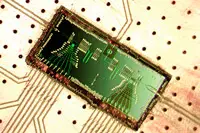 What is said to be a major step forward in the development of quantum computing systems has been made by researchers at Princeton University in the US. The team has built a laser the size of a grain of rice powered laser powered by single electrons tunnelling through quantum dots. The microwave laser (maser) is said to demonstrate the fundamental interactions between light and moving electrons.
The original aim of the project was not to build a maser, but to explore how to use double quantum dots as quantum bits. Because quantum dots can communicate through the entanglement of light particles, or photons, the researchers designed dots that emit photons when single electrons leap from a higher energy level to a lower energy level to cross the double dot.
Each double quantum dot can only transfer one electron at a time, said Jason Petta, an associate professor of physics. "It is like a line of people crossing a wide stream by leaping onto a rock so small that it can only hold one person," he said. "They are forced to cross the stream one at a time. These double quantum dots are zero-dimensional as far as the electrons are concerned – they are trapped in all three spatial dimensions."
The researchers fabricated the double quantum dots from 50nm diameter indium arsenide nanowires. These were patterned over smaller metal wires that act as gate electrodes.
When the device was switched on, electrons flowed single-file through each double quantum dot, causing them to emit photons in the microwave region of the spectrum. These photons then bounced off mirrors at each end of the cavity to build into a coherent beam of microwave light.
The device demonstrates a major step forward for efforts to build quantum computing systems out of semiconductor materials, according to Jacob Taylor, an adjunct assistant professor at the Joint Quantum Institute, University of Maryland-National Institute of Standards and Technology. "I consider this to be a really important result for our long term goal, which is entanglement between quantum bits in semiconductor-based devices."
One advantage of the new maser is that the energy levels inside the dots can be fine-tuned to produce light at other frequencies, something not possible with other semiconductor lasers.
Author
Graham Pitcher
Source: www.newelectronics.co.uk
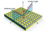 A team of electrical engineers from Penn State University in the US has developed a device featuring a single layer of metallic nanostructures and says the device provides 'exceptional capabilities' for manipulating light. Applications potentially include satellite communications.
"We have designed and fabricated a waveplate that can transform the polarisation state of light," said post doctoral fellow Zhi Hao Jiang. "Polarisation is one of the most fundamental properties of light. For instance, if we transform linearly polarised light into circularly polarised light, this could be useful in optical communication and biosensing."
While thin waveplates have been demonstrated previously, they had an average power efficiency of less than 50%. Penn State's nanofabricated waveplate is said to achieve polarisation conversion rates of more than 92% over a bandwidth of more than an octave and with a 40° field of view.
"We demonstrated with simulation and experiment both quarter- and half-waveplate metasurfaces that operate in the visible spectrum as well as in the near infrared," said researcher Jeremy Bossard. "It also has a wide field of view, which means that if you illuminate the surface from a wide range of angles, it would still give the same reflective performance." A wider field of view can reduce the number of optical components in a system and achieve wide broadband functionality in the visible to near infrared wavelength range.
Author
Graham Pitcher
Source: www.newelectronics.co.uk
 A new generation of outdoor displays is being developed by Austrian company Trilite Technologies, in conjunction with scientists from the Vienna University of Technology.
The approach uses a sophisticated system to send laser beams in different directions. The angular resolution of the system is said to be so fine that the left eye sees a different picture than the right one, creating a 3D effect.
The system is based on a module called a 'trixel'. This comprises lasers and a moveable mirror. "The mirror directs the laser beams across the field of vision, from left to right. During that movement the laser intensity is modulated so that different laser flashes are sent into different directions," said Professor Ulrich Schmid of Vienna University of Technology.
Together, TriLite and TU Vienna have created the first prototype. Although it only has a resolution of five pixels by three, it shows the system works. A second prototype, which will display colour images at higher resolution, is in development. TriLite says the system will also be tunable to suit the location.
Such electronic billboards might also display different ads, seen from different angles. "Maybe someone wants to appeal specifically to the customers leaving the shop across the street, while a different ad is shown to people waiting at a bus stop," said Ferdinand Saint-Julien, TriLite's CEO. "Technically, this would not be a problem."
Author
Graham Pitcher
Source: www.newelectronics.co.uk
 Materials scientists at University of Wisconsin-Madison say they have made a significant leap towards the creation of electronics with improved battery life and the ability to flex and stretch.
The team, led by materials science Associate Professor Michael Arnold, pictured, and Professor Padma Gopalan, has reported the highest performing carbon nanotube transistors yet demonstrated, with an on-off ratio 1000 times better and 100 times better conductance than the previous best carbon nanotube transistors.
"Carbon nanotubes are very strong and very flexible, so they could also be used to make flexible displays and electronics that can stretch and bend, allowing you to integrate electronics into new places, like clothing," said Arnold. "The advance enables new types of electronics that aren't possible with the more brittle materials manufacturers are currently using."
Drawing on more than two decades of carbon nanotube research, the team used a technique called floating evaporative self assembly to create a solution of ultra high purity semiconducting carbon nanotubes.
The development is also said to bring closer the day when carbon nanotube transistors might be a feasible replacement for silicon transistors in processors and high frequency communication devices.
"This is not an incremental improvement in performance," Arnold claimed. "With these results, we've really made a leap in carbon nanotube transistors. Our carbon nanotube transistors are an order of magnitude better in conductance than the best thin film transistor technologies currently being used commercially, whilst still switching on and off like a transistor is supposed to function."
Author
Graham Pitcher
Source: www.newelectronics.co.uk