Electronics News
Archive : 20 January 2015 год
 A new signal amplification process discovered by a team from the University of California, San Diego is poised to underpin new generations of electrical and photonic devices, according to the researchers.
"For many years, the semiconductor industry has relied on photodetectors for optoelectrical conversion, followed by low noise electronic amplifiers to convert optical signals into electronic signals with amplification to enable information detection and processing," explained Yu-Hwa Lo, Professor of electrical and computer engineering at the University.
The highest sensitivity has been achieved by combining an electronic amplifier with a photodetector that uses an internal amplification mechanism to balance out the thermal noise of the electronic amplifier and shot noise in the photodetector.
"Avalanche photodetectors that use impact ionisation became the devices of choice and have remained so for many decades," Prof Lo continued. However, impact ionisation has its drawbacks, so the team searched for a more efficient intrinsic amplification mechanism that would work at lower voltage and noise than the current method.
"We've discovered a far more efficient mechanism – the cycling excitation process (CEP) – to amplify the signal," Prof Lo noted.
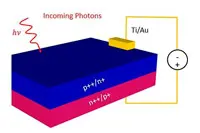
The device primarily has a p/n junction similar to that found in a semiconductor device. "The only unique feature is that both sides of the p/n junction contain a substantial amount of counter doping – a large number of donors exist in the p-region, with acceptors in the n-region," Prof Lo explained.
Counter impurities in the compensated p/n junction enable the highly efficient amplification process. Electrons or holes crossing the depletion region gain kinetic energy and, in turn, excite new electron-hole pairs using the compensating impurities as intermediate states.
With further improvements, says the team, the mechanism can be used in a variety of devices and semiconductors.
"With an efficient gain mechanism at an operation voltage compatible with CMOS integrated circuits, it's possible to produce communication and imaging devices with superior sensitivity at a low cost," Prof Lo concluded.
Author
Graham Pitcher
Source: www.newelectronics.co.uk
 Telesoft Technologies has selected Achronix' Speedster22i HD1000 FPGAs for use in its MPAC6200 dual 100GbE PCIe card for cyber security, monitoring and analytics.
"Use of Speedster22i FPGAs has accelerated our product development cycle time," said Rob Downham, Telesoft's chairman. "In previous FPGA projects, the integration of 100G Ethernet, Interlaken, PCI Express Gen3 and DDR3 soft IP blocks took many months of effort that was not required with the Achronix solution. We also gained back 50% of the logic fabric as the soft IP was moved to Speedster22i hard IP."
Based on Intel's 22nm Tri-Gate technology, Speedster22i devices contain a range of embedded hard IP and this, together with 86Mbit of on-chip memory, were said to be key aspects in Telesoft's selection of the Speedster22i device.
"We are delighted to be partnering with Telesoft Technologies," said Achronix' CEO Robert Blake, pictured. "The embedded hard IP in Speedster22i HD FPGAs eliminates the cost of purchasing, integrating, closing timing and testing the functions that are required when soft IP is used."
Author
Graham Pitcher
Source: www.newelectronics.co.uk
 York EMC Services has opened a new compliance test laboratory, relocating its Scottish operation from Dalgety Bay to Grangemouth. The purpose built laboratory offers a range of EMC, safety, radio, telecoms and EMF compliance services to companies in Scotland and the North of England.
Chief Executive Nick Wainwright said: "The compliance industry is constantly changing, which means we need to evolve to make sure that we continue to meet the needs of our customers. The convenient location of our Grangemouth laboratory with its brand new facilities, not to mention the key expertise of our experienced team, will ensure that we are uniquely placed to add value to businesses in Scotland and the North of England."
The facility features new EMC test chambers, including a fully compliant 3m semi anechoic/fully anechoic chamber, enabling radiated emissions to be performed in an electromagnetically quiet environment. This chamber, the first in the UK, has been built using DuraSorb, a lightweight, high performance absorber.
Author
Graham Pitcher
Source: www.newelectronics.co.uk
 The emission of light from and capture of light by metamaterials can be enhanced with the use of light emitting nanocrystals, according to research conducted by the City College of New York, along with scientists from the University of Alberta and Purdue University. The work is believed to have application in ultrafast LEDs, nanoscale lasers and single photon sources.
The team used metamaterials with hyperbolic dispersion to enhance the light emission properties of the nanocrystals and simultaneously engineered an efficient light extraction scheme.
"The idea of metamaterials in the context of optics is that you can manipulate light and decide how you want it to behave in this medium," said City College photonics expert Professor Vinod Menon.
Enhancement in light emission from metamaterials has been demonstrated in the past by several groups, but the results were said to not be useful since light was not emitted readily. The latest work is said to overcome this issue and to take the first step towards practical metamaterial based light emitters.
"We've shown both an increase in light emission and [the ability] to extract light," added Prof Menon.
Author
Graham Pitcher
Source: www.newelectronics.co.uk
 Light communication company pureLiFi – previously known as pureVLC – has raised £1.5million in its latest round of investment as it ships Li-Flame, what is said to be the world's first full wireless LiFi networking system.
The latest investors in the University of Edinburgh spin off were led by London and Scottish Investment Partners, the Scottish Investment Bank and Old College Capital.
Professor Russel Griggs, pureLiFi's chairman, said: "I am very pleased that the necessary funding is now in place to allow Harald Haas and his team to push ahead with the product roadmap, positioning pureLiFi for its next phase of growth."
Harald Haas, pictured, pureLiFi's cofounder and chief scientific officer, added: "LiFi is increasingly viewed as a transformative technology that can change the way we use the mobile internet as part of future 5G cellular networks and at the same time be an enabler of the emerging Internet of Things."
Author
Graham Pitcher
Source: www.newelectronics.co.uk
 Scientists at Imperial College London have developed a way to manipulate the optical properties of polymers by drawing patterns with a solvent 'ink'. The approach is said to allow more precise control over how these materials interact with light and could have application in all kinds of devices that emit, detect and control light. One example offered by the research team is the ability to make tiny LEDs that emit light in one direction only, rather than across a broad range of angles, thereby offering the prospect of compact light source arrays for medical diagnostic applications.
The researchers used a tiny pen to draw patterns with a solvent on a thin film of polymer semiconductor. The solvent changes the shape of a selection of chain segments from a disordered state to ordered rigid strands. This change in structure alters the way in which the material interacts with light, changing its refractive index as well as the colour of light emitted.
Professor Donal Bradley, director of the Centre for Plastic Electronics at Imperial College London, said: ",Usually we use lenses or mirrors to change the direction of light. This method lets us manipulate a light source itself to tightly control the direction of light that it emits. The material adopts the desired structure naturally – it just requires a little encouragement to do so."
The approach is said to allow scientists to alter these properties on a much smaller scale than they could before – over distances shorter than the wavelength of light. The researchers expect this will make it possible to build a variety of novel structures leading to new and more efficient devices.
Author
Graham Pitcher
Source: www.newelectronics.co.uk
 Intersil has launched the ISL8203M, a dual 3A/single 6A step down DC/DC power module said to simplify the design of power supplies for FPGAs, ASICs, microprocessors and DSPs.
The module is described as a complete encapsulated power system featuring a PWM controller, synchronous switching MOSFETs, inductors and passive components. Accepting an input in range from 2.85V to 6V, the device has an output adjustable between 0.8V and 5V. This, says the company, allows designers to use one device to build a single 6A or dual output 3A power supply.
"Our customers are building increasingly compact DC/DC solutions," said Mark Downing, senior vice president of Infrastructure and Industrial Power Products at Intersil. "The ISL8203M analog power module offers the smallest footprint for a dual output low power solution without performance compromise, making it possible for customers to get the footprint and the efficiency they require."
Supplied in a QFN package measuring 9 x 6.5mm, the module is said to have an efficiency of 95%.
Author
Graham Pitcher
Source: www.newelectronics.co.uk
 An international research team, including scientists from Forschungszentrum Jülich and the Paul Scherrer Institute in Switzerland, has created the first semiconductor laser consisting solely of Group IV elements.
The germanium-tin (GeSn) laser can be applied directly onto a silicon chip and thus creates a new basis for optical data transmission. "Signal transmission via copper wires limits the development of larger and faster computers due to the thermal load and the limited bandwidth of copper wires," said Professor Detlev Grützmacher, director of Jülich's Peter Grünberg Institute. "The clock signal alone synchronising the circuits uses up to 30% of the energy – energy which can be saved through optical transmission."
Typical semiconductor lasers for telecommunication systems are made from Group III-V elements – gallium arsenide for example and are costly and cannot be applied directly onto silicon. However, Group IV semiconductors – which includes silicon and germanium – can be integrated into standard manufacturing processes.
The scientists have created the semiconductor laser by combining germanium and tin – another Group IV element. "The high tin content is decisive for the optical properties," said PhD students Stephan Wirths. "For the first time, we were able to introduce more than 10% tin into the crystal lattice without it losing its optical quality."
According to the team, the Ge-Sn laser emits light with a wavelength of about 3µm and this may also allow its use in applications such as carbon compound detection.
Author
Graham Pitcher
Source: www.newelectronics.co.uk
 Ambiq Micro has launched the Apollo family and claims the parts – which feature a 32bit ARM Cortex-M4F microcontroller core – have an energy consumption typically 5 to 10 times less than than that of MCUs with comparable performance.
The devices use the company's patented Subthreshold Power Optimized Technology (SPOT) platform to run transistors at subthreshold voltages of less than 0.5V.
Mike Salas, vp of marketing, noted the concept of subthreshold processing has been around since the 1970s. "Then, designs were hand crafted, with very few transistors. It wasn't until 2005 that people started to see if there were ways to commercialise the approach when using millions of transistors."
SPOT uses the leakage current of 'off' transistors to compute in both digital and analogue domains. The technology, which uses a standard CMOS process, is said to have overcome such challenges as noise susceptibility, temperature sensitivity and process drift.
"Instead of using 1.8V, for example," said Salas, "we toggle down to 0.5V. Because energy is proportional to V2, we get a big improvement in power. Adaptive circuitry that sits on the silicon deals with issues in the analogue and digital domains, such as extracting the signal from noise."
Apollo users can optimise the performance of active and sleep modes at the same time, said Salas. "With other MCUs, you have to choose one or the other. Sleep mode can be optimised using an older process node, but that is at the expense of dynamic power. Or you could use a newer technology, but that has higher leakage."
Because of the reduction in power consumption, it becomes feasible to integrate a Cortex-M4F core, rather than the Cortex-M0+ found in other low power MCUs. This is said to make the part attractive for use in wearable electronics.
The Apollo MCUs run at up to 24MHz – the 'sweet spot', according to Salas – and are available with up to 512kbyte of flash and 64kbyte of RAM. Alongside I2C/SPI ports and a UART, resources include a 10bit, 13 channel A/D converter running at 1Msample/s and a temperature sensor with an accuracy of ±2ºC. Two packaging options are available – a 64pin BGA measuring 4.5 x 4.5mm and a 42pin CSP measuring 2.4 x 2.77mm.
Author
Graham Pitcher
Source: www.newelectronics.co.uk

