
Electronics News
Archive : 10 October 2015 год
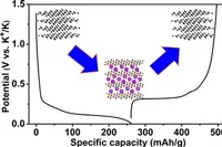 Research at Oregon State University has shown that potassium can work with graphite in a potassium-ion battery; a discovery which may pose a challenge and sustainable alternative to the lithium ion battery.
According to the research team, potassium ion batteries were last explored in 1932. “For decades, people have assumed that potassium couldn’t work with graphite or other bulk carbon anodes in a battery,” said Xiulei Ji, assistant professor of chemistry. “That assumption is incorrect. It’s really shocking that no one ever reported on this issue for 83 years.”
The findings are of considerable importance, the researchers say, because of lithium’s relative rarity – found in only 0.0017%, by weight, of the Earth’s crust. However, researchers have yet to duplicate its performance with less costly and more readily available materials.
The Oregon team’s work shows that that potassium – 880 times more abundant than lithium – can work effectively with graphite or soft carbon in the anode of an electrochemical battery. While the performance is not equivalent to that of lithium-ion batteries, improvements in technology should narrow the gap, said Ji.
“It’s safe to say that the energy density of a potassium-ion battery may never exceed that of lithium-ion batteries,” he said. “But they may provide a long cycling life, a high power density, lower cost and be ready to take advantage of the existing manufacturing processes of carbon anode materials.”
Author
Graham Pitcher
Source: www.newelectronics.co.uk
 Looking to meet growing demand for more performance from video processing systems, but with lower energy consumption, Cadence has unveiled the Tensilica Vision P5 digital signal processor (DSP).
The flagship imaging and vision core is said to offer up to 13X better performance than the company’s previous generation device while consuming five times less energy on vision tasks.
Dennis Crespo, director of product marketing for Cadence’s Tensilica group, said: “Cameras are everywhere. While Tensilica has a long history of working with mobile apps, these have mainly been ‘close to camera’. We are now expanding into automotive with this new generation, looking to target vision applications inside and outside of the vehicle.”
The Vision P5 has been developed for applications requiring high memory and operation parallelism, supporting complex vision processing at high resolution and frame rates. Suitable for offloading vision and imaging functions from the main CPU, the device is likely to find application in such areas as image and video enhancement, robotic vision, and face detection and authentication. Other potential applications include object tracking and object avoidance.
“With smaller pixels in cameras,” Crespo noted, “there are more problems to be solved, including noise. Different sensors have different noise patterns, so a DSP is needed for correction, as well as to perform tasks like image stabilisation. Meanwhile, face detection requires depth sensing, which also needs a DSP.”
The core features: a 1024bit memory interface with SuperGather technology; up to four vector ALU operations per cycle, each with up to 64way data parallelism; up to five instructions issued per cycle; an enhanced 8,16 and 32bit ISA tuned for vision/imaging applications; and an optional 16 way IEEE single precision vector floating point processing unit delivering 32GFLOPs at 1GHz.
Crespo said the device can handle 256 ALU operations per cycle, compared to the previous 90, and features 430 additions to the instruction set.
“We have a customer who plans to use an eight core version of the P5, consuming less than 4W, in a scientific computing application,” said Crespo. “This will replace a GPU array consuming 250W.”
According to the company, the P5 can run at clock speeds of 1.1GHz when targeted at a 16nm FinFET process.
Author
Graham Pitcher
Source: www.newelectronics.co.uk
 Researchers at the University of Rochester, New York have succeeded in shrinking photonic devices below the diffraction limit of visible light - around 200 to 300nm - a necessary step on the road to making photonic circuits competitive with today's technology. The scientists developed a nanoscale photodetector that uses molybdenum disulphide to detect optical plasmons and demonstrated that light can drive a current using a silver nanowire.
Kenneth Goodfellow, a graduate student in the laboratory of the Quantum Optoelectronics and Optical Metrology Group, said: "It is a step towards using light to drive, or, at least complement electronic circuitry for faster information transfer."
The device expands on previous work demonstrating that light could be transmitted along a silver nanowire as a plasmon and re-emitted at the other end, which was covered with atomically-thin flakes of molybdenum disulfide (MoS2). When re-emitted, the light corresponded to the band gap of MoS2, rather than solely to the laser's wavelength, demonstrating that the plasmons effectively nudged the electrons in MoS2 into a different energy state.
"The natural next idea would be to see if this type of device would be able to be used as a photodetector," Goodfellow said.
To do this, the group transferred a silver nanowire coated at one end with MoS2 onto a silicon substrate and deposited metal contacts onto that same end with electron beam lithography. They then connected the device to equipment to control its bias, or fixed, voltage and to measure the current running through it.
When the uncovered end of the wire was exposed to a laser, the energy was converted into plasmons. This energy electronically excited an electron once it reached the molybdenum disulphide-covered end, effectively generating a current.
"Full photonic circuits are some way off in the future, but this work helps to feed the current effort," Goodfellow said.
Future work for the group includes reducing potential contamination in device assembly by transitioning to a complete dry transfer of wires and MoS2 onto prefabricated electrodes, as well as gaining better control of the MoS2 doping process to add additional charge carriers and improve the device's efficiency.
Pic: This image shows light traveling along a silver nanowire as plasmons and re-emitted via molybdenum disulphide
Author
Tom Austin-Morgan
Source: www.newelectronics.co.uk