
Electronics News
Archive : 11 October 2015 год
 Qualcomm Technologies has demonstrated a Server Development Platform (SDP), which the company says is sampling to Tier 1 data centres. The system includes a pre production version of 24 core SoC based on the ARMv8-A instruction set.
“The release of our evaluation system is a major milestone for Qualcomm Technologies. As data centres evolve to support the exponential growth and innovation in data, connectivity and cloud services, Qualcomm is creating an ecosystem to meet the needs of these next generation data centres with Qualcomm-based server technologies,” said Anand Chandrasekher, senior vice president.
Targeted at hyperscale data centres, Qualcomm Technologies’ server SoC technology is designed to tackle common workloads, including Infrastructure as a Service, Platform as a Service, big data and machine learning. The 24 core SoC has been built on an advanced FinFet process and is said to integrate standard server class features, including PCIe and storage.
Meanwhile, Qualcomm has signed deals with Mellanox and Xilinx, for Ethernet and InfiniBand interconnect and FPGA enabled dynamic workload acceleration respectively.
In November 2014, Qualcomm announced plans to develop ARM based chips targeted at data centres. At the time, CEO Steve Mollenkopf described the server market as ‘an interesting opportunity’ and noted: “We will have a server product. Qualcomm's road map at the high end is merging with what is feasible to put into a data centre.”
Author
Graham Pitcher
Source: www.newelectronics.co.uk
 An £11million research programme to develop fully autonomous cars, ‘Towards Autonomy - Smart and Connected Control’, is being jointly funded by the Engineering and Physical Sciences Research Council (EPSRC) and Jaguar Land Rover (JLR).
The research, which will take place at ten UK universities and the Transport Research Laboratory, was announced by Secretary of State for Business, Sajid Javid during a visit to JLR’s facility at Gaydon in Warwickshire.
Five projects have been selected and JLR will be leading the collaboration with these research groups.
“To realise the future potential for fully autonomous vehicles, we need to give drivers, pedestrians and other road users the confidence that a car driving around with little or no human input is a safe, viable and rewarding experience,” Dr Wolfgang Epple, director of research and technology, JLR, said. “These collaborative projects will bring some of the UK’s leading academics together with our autonomous driving team to address the fundamental real-world challenges that are part of our journey towards autonomous driving.”
The projects will look into the use of radar and video sensing to interpret the external environment, road conditions and other road users; how drivers will react to new autonomous systems; how systems can be designed to adapt to the personal characteristics of users; investigate how the transition between human control and automated systems can be designed to best effect; how distributed control systems and cloud computing can be integrated with vehicles; and how data from intelligent infrastructure, drivers and automated vehicles can be used to aid interaction.
Professor Philip Nelson, EPSRC’s chief executive, said; “Science and engineering research is vital to technological innovation and to keeping UK businesses at the forefront of global markets. This joint investment shows how strategic partnerships between the research councils, universities and business can identify industry’s challenges and build the academic expertise needed to meet them.”
Author
Tom Austin-Morgan
Source: www.newelectronics.co.uk
 A team of Australian engineers at the University of New South Wales (UNSW), in Sydney, has taken the first step towards making quantum computers a reality by building a quantum logic gate in silicon for the first time.
“What we have is a game changer,” said team leader Andrew Dzurak, Scientia Professor and director of the Australian National Fabrication Facility at UNSW. “We’ve demonstrated a two-qubit logic gate – the central building block of a quantum computer – and, significantly, done it in silicon. Because we use essentially the same device technology as existing computer chips, we believe it will be much easier to manufacture a full-scale processor chip than for any of the leading designs, which rely on more exotic technologies.
“This makes the building of a quantum computer much more feasible, since it is based on the same manufacturing technology as today’s computer industry,” he added.
In classical computers, data is rendered as binary bits, which are always in one of two states: 0 or 1. However, a quantum bit (qubit) can exist in both of these states at once, a condition known as a superposition.
Until now, it had not been possible to make two qubits interact with each other using silicon. But the UNSW team, working with Professor Kohei M. Itoh of Japan’s Keio University, has done just that for the first time.
The result means that all of the physical building blocks for a silicon-based quantum computer have now been constructed, allowing engineers to begin the task of designing and building a functioning quantum computer.
The team has patented a design for a full-scale quantum computer chip that would allow for millions of qubits, all doing the types of calculations that it has experimentally demonstrated. According to Dzurak, the next step for the project is to identify the right industry partners to work with to manufacture the full-scale quantum processor chip.
A full-scale quantum processor would have major applications in the finance, security and healthcare sectors, allowing the identification and development of new medicines by greatly accelerating the computer-aided design of pharmaceutical compounds, and minimising lengthy trial and error testing; the development of new, lighter and stronger materials; and faster information searching through large databases.
Pic: Andrew Dzurak, director of the Australian National Fabrication Facility at UNSW
Author
Tom Austin-Morgan
Source: www.newelectronics.co.uk
 A professor of theoretical physics and condensed matter theory from Caltech has suggested that a new type of quasiparticle could help improve the efficiency of photonic devices.
While electrons travelling through semiconductors lose energy via heat because of resistance, a similar effect can be seen with light transmission, caused by factors such as unwanted reflection and photon scattering. Prof Gil Refael says a quasiparticle called the ‘topolariton’ could reduce such signal degradation and enhance the stability of the photons as they move along the edges of semiconductors.
The topolariton is described as an emergent particle: one that exhibits some, but not all, of the characteristics of elementary particles. Examples include phonons, solitons and excitons.
When photons and excitons interact, they can form polaritons and the topolariton is said to be a type of polariton that can flow in one direction along the edges of semiconducting quantum wells embedded in optical cavities.
Because topolaritons are part matter and part light, Prof Refael suggests they could be guided and controlled with reflectors or with photonic band-gaps. However, the professor admits it might take some time before practical applications are seen. “We’ll need to create some new interfaces between the photonic and electronic worlds,” he said.
Pic: Credit: T Karzig et al
Author
Graham Pitcher
Source: www.newelectronics.co.uk
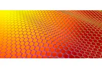 The Centre of Process Innovation (CPI) has announced that it has joined a UK based collaboration called ‘Gravia’, to develop the next generation of ultra-barrier materials using graphene for the production of flexible transparent plastic electronic based displays for the next generation of smartphones, tablets and wearable electronics.
The graphene market is predicted to be worth more than £800million by 2023 and could transform the manufacturing landscape in the UK.The project, including the University of Cambridge, FlexEnable and the National Physical Laboratory (NPL), expects to deliver a feasible material and process system. It builds upon existing investments by Innovate UK and the EPSRC in this area.
“The collaboration brings together world class supply chain expertise across the UK to bridge the gap from Graphene research to the manufacturing of commercial flexible display screens,” said James Johnstone, business development manager at CPI. “CPI’s role in the project is to use roll-to-roll atomic layer deposition technologies to scale up, test and fabricate the ultra barrier materials.”
The incorporation of graphene interlayers offers potential for flexible displays. Its gas blocking properties will enable barrier materials that are flexible, transparent, robust, and impervious to many molecules. Gravia will seek to accelerate product development, improving upon current ultra barrier performance and lifetimes by producing consistent barrier materials and processes on large area substrates by utilising specialist growth techniques. The key challenge will be to develop large-area poly-crystalline graphene films which maximise performance whilst mitigating process imperfections.
The demonstration of feasible working prototypes will represent an achievement in the race to bring wearable electronics and plastic displays to the mass market. The project is exploring the necessary industrial process parameters to ensure that the barriers produced feature high performance at a price point that allows market adoption.
Future development work will focus on transferring the technology from proof of concept to pilot production scale.
Author
Tom Austin-Morgan
Source: www.newelectronics.co.uk
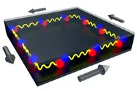
 A research team, including scientists from the National Institute of Standards and Technology (NIST), has developed a straightforward method to create magnetic skyrmions under ambient room conditions. The achievement brings skyrmions a step closer for use in data storage and could be the basis for a new type of computer memory that never loses the data it stores.
Skyrmions are not fundamental pieces of matter; they are effects named after the physicist who proposed them. Until just recently, magnetic skyrmions had only been seen at very low temperatures and under powerful magnetic fields.
The magnetic force in each individual atom in a magnet - what physicists call their ‘magnetic moments’ - all line up the same way, like tiny compasses all pointing in the same direction. But under extreme conditions, certain magnetic materials can develop spots where the moments curve and twist, forming a ring-like configuration. These unusual objects possess an elasticity that protects them from outside influence, meaning the data they store would not be corrupted easily, even by stray magnetic fields or physical defects within the material. As a result, magnetic skyrmions present a promising basis for information memory systems and other nanoelectronic devices.
A hurdle in using traditional skyrmions was the extreme lab conditions needed to form them. While NIST's Dustin Gilbert was a graduate student at the University of California, Davis, he designed an approach to make the quantum objects remain stable at room temperature with no magnetic field.
Creating skyrmions involves placing arrays of tiny magnetised cobalt disks on top of a thin film made of cobalt and palladium; the NIST Centre for Neutron Research (NCNR) had just developed a state-of-art polarised neutron reflectometer that was well suited to study Gilbert’s lab results. Working with NCNR scientists, the team used neutrons to see through the disk to spot the skyrmions underneath. The team also captured images of the whirling configurations in the disk array at NIST's Centre for Nanoscale Science and Technology and Lawrence Berkeley Laboratory.
"The idea that has been discussed is that you could push these stable magnetic bundles in single file down a line and read their data. The advantage here is that you'd need way less power to push them around than any other method proposed for spintronics," says Gilbert. "What we need to do next is figure out how to make them move around. But for now, we can start exploring how we might use skyrmions in technology."
Pic: A magnetized cobalt disk (red) placed atop a thin cobalt-palladium film (light purple background) can be made to confer its own ringed configuration of magnetic moments (orange arrows) to the film below, creating a skyrmion in the film (purple arrows)
Author
Tom Austin-Morgan
Source: www.newelectronics.co.uk
 Renesas Electronics has announced the ADAS Surround View Kit. An extension of the ADAS Starter Kit, the Surround View Kit is said to simplify and accelerate the development of surround view applications when combined with the Starter Kit.
The ADAS Surround View Kit combines automotive cameras from Integrated Micro-electronics and multiple high-speed gigabit multimedia serial links (GMSL) from Maxim Integrated Products on a miniature automotive chassis. This is said to eliminate the need for system manufacturers to source and set up these components themselves for their surround view development.
The kit provides a 2-channel CAN interface and a gigabit Ethernet connector interface for in-car applications, where the model chassis is not used.
Once connected via an on-board extension connector to the ADAS Starter Kit, the ADAS Surround View Kit is claimed to provide outstanding processing performance to system manufacturers. It is based on the cutting-edge performance of Renesas’ R-Car H2 SoC, which is capable of delivering more than 25,000 DMIPS and providing state-of-the-art 3D graphics capabilities and powerful vision processing cores. The R-Car H2 SoC supports up to four independent input HD camera channels, allowing the implementation of 360° camera views and object recognition.
The kit is supported by the Yocto distribution that is also used for other R-Car evaluation boards. In addition, Renesas will provide sample applications that will help system manufacturers to use the ADAS Surround View Kit, and accelerate the development of dedicated hardware and software solutions for future ADAS applications.
Author
Tom Austin-Morgan
Source: www.newelectronics.co.uk
 Skyworks Solutions is to acquire PMC-Sierra in a $2billion cash deal. According to Skyworks, the deal enhances its position as a diversified analogue, RF and mixed signal semiconductor provider.
“With our acquisition of PMC, Skyworks will be [well] positioned to capitalise on the explosive demand for high performance solutions that seamlessly connect, transport and store Big Data,” said David Aldrich, Skyworks’ chairman and CEO. “Specifically, we plan to leverage PMC’s innovative storage systems, flash controllers, optical switches and network infrastructure solutions to expand our engagements with some of the world’s leading OEMs and ODMs, as well as emerging hyperscale data centre customers.
“At a higher level, this complementary … acquisition is consistent with our stated strategy of diversifying into adjacent vertical markets while leveraging our system-level expertise and global scale.”
With an expanded product portfolio, customer base and end market applications, Skyworks expects its annual revenues to grow to around $4bn from the current level of $2.3bn.
Greg Lang, president and CEO of PMC, noted: “Together, we plan to develop a wider range of leading edge solutions for our customers, target new growth vectors and enable some of the most exciting networking and storage platforms in the world.”
Since its establishment in 2002, Skyworks has made a number of acquisitions, including analogue specialist Advanced Analogic Technologies and RF front end specialist SiGe Semiconductor.
Author
Graham Pitcher
Source: www.newelectronics.co.uk
 Sony has announced plans to split its devices business into three new companies, addressing semiconductors, batteries and storage solutions. The three units will all report to Sony’s executive deputy president and corporate executive officer Tomoyuki Suzuki. The move is intended to improve accountability and to allow the new companies to react more quickly to market developments.
Semiconductor interests – primarily image sensors – will be handled by Sony Semiconductor Solutions, with R&D, business control, sales and other activities transferred in by April 2016.
In the battery business, Sony Energy Devices will target opportunities in the growing battery market, along with enhancing its ability to generate a profit. Meanwhile, Sony Storage Media and Devices – currently a manufacturing operation – will inheret business related functions.
Sony has been struggling over the last few years and has spun out its audio/video business, as well as its TV and PC operations. Unlike these businesses, the semiconductor business has contributed significantly to Sony’s revenues.
Brian O’Rourke, senior principal analyst, consumer devices and MEMS and sensors, with IHS, noted: “Sony is obviously moving in a new direction, in order to ease planning, shorten time to market and increase profitability. What will the ultimate effect of this spin out have on Sony’s image sensor business?
He notes Sony has been ‘wildly successful’ in the image sensor market, where it holds a 42% market share. “What will the ultimate effect of this spin out have on Sony’s image sensor business?,” he asks.
Author
Graham Pitcher
Source: www.newelectronics.co.uk
 Belgian nanoelectronics research centre imec and Cadence Design Systems have completed the first tapeout of a 5nm test chip, created using a mixture of extreme ultraviolet (EUV) and 193nm immersion lithography techniques.
The partners say they optimised design rules, libraries and place and route technology to obtain optimal power, performance and area scaling using Cadence’s Innovus Implementation System.
“Our collaboration with Cadence plays an important part in the development of the world’s most advanced geometries, including 5nm and below,” said An Steegen, imec’s senior vice president of process technology.
The test chip, based on a processor design, not only used EUV lithography. but also self-aligned quadruple patterning at 193nm. In the latter process, metal pitches were scaled to 24nm in order to push the limit of patterning.
“By achieving this milestone, Cadence and imec continue to demonstrate our dedication toward pushing patterning technologies to increasingly smaller nodes,” said Dr Anirudh Devgan, general manager of Cadence’s Digital and Signoff Group.
Author
Graham Pitcher
Source: www.newelectronics.co.uk