
Electronics News
Archive : 16 October 2015 год
 Researchers at New York State’s Binghamton University have demonstrated an eco-friendly process that enables unprecedented spatial control over the electrical properties of graphene oxide.
By using the probe of an atomic force microscope to trigger a local chemical reaction, Jeffrey Mativetsky, assistant professor of physics at Binghamton University, and PhD student Austin Faucett showed that electrically conductive features as small as 4nm can be patterned into individual graphene oxide sheets.
Mativetsky said: "Unlike standard methods for manipulating the properties of graphene oxide, our process can be implemented under ambient conditions and is environmentally-benign, making it a promising step towards the practical integration of graphene oxide into future technologies."
The study provides new insight into the spatial resolution limits and mechanisms for a relatively new process for patterning conductive regions in insulating graphene oxide. The minimum conductive feature size of 4nm is the smallest achieved so far by any method for this material.
This research not only enables fundamental study of the nanoscale physical properties of graphene oxide but also opens up new avenues for incorporating graphene oxide into future technologies. Because the process developed by Mativetsky avoids the use of harmful chemicals, high temperatures or inert gas atmospheres, his work represents a promising step towards environmentally-friendly manufacturing with graphene oxide.
"At first, this will mainly be useful for studying fundamental properties and lab-scale devices," said Mativetsky. "Eventually, this work may help lead to the practical integration of graphene oxide into low-cost and flexible electronics, solar cells, and sensors.”
Pic: Jeffrey Mativetsky, assistant professor of physics at Binghamton University
Author
Tom Austin-Morgan
Source: www.newelectronics.co.uk
 Cadence Design Systems has announced that Phison Electronics Corporation has used the Cadence Voltus-Fi Custom Power Integrity Solution to achieve silicon-proven accuracy on electromigration and IR-drop (EMIR) checks for its flash controller chips. Phison claims the tool reduced its tapeout schedule by eight weeks, improving time to market by 40% while also increasing overall product reliability.
The Voltus-Fi Custom Power Integrity Solution is a transistor-level EMIR tool that is said to deliver foundry-certified SPICE-level accuracy in power signoff.
The Phison design team says it delivered three proven silicon designs in 12 months by coupling the Voltus-Fi with the Virtuoso custom design platform. The Cadence tool suite provided the design team with circuit simulation and layout EMIR analysis, debugging and fixing to improve overall design productivity.
“Using a low-power design methodology and maintaining power-grid integrity have become critical design requirements for signoff, especially at lower process nodes,” said Aw Yong Chee Kong, president at Phison Electronics. “By incorporating the Cadence Voltus-Fi Custom Power Integrity Solution into our design flow, Phison engineers have been able to find design weaknesses such as potential voltage drop and electromigration failures, preventing costly silicon re-spins.”
Author
Tom Austin-Morgan
Source: www.newelectronics.co.uk
 A research team from the University of Wisconsin-Madison (UW) and the US Department of Energy's Argonne National Laboratory has developed a way to control the growth paths of graphene nanoribbons on the surface of a germanium crystal.
"Researchers have wanted to make transistors out of carbon nanotubes but the problem is that they grow in all sorts of directions," said Brian Kiraly of Argonne. "The innovation here is that you can grow these along circuit paths that works for your tech."
UW researchers used chemical vapour deposition to grow graphene nanoribbons on germanium crystals. This technique passes a mixture of methane, hydrogen and argon gases into a tube furnace. At high temperatures, methane decomposes into carbon atoms that settle onto the germanium's surface to form a uniform graphene sheet. By adjusting the chamber's settings, the UW team was able to exert precise control over the material.
"What we've discovered is that when graphene grows on germanium, it naturally forms nanoribbons with these very smooth, armchair edges," said Michael Arnold, an associate professor of materials science and engineering at UW-Madison. "The widths can be very, very narrow and the lengths of the ribbons can be very long, so all the desirable features we want in graphene nanoribbons are happening automatically with this technique."
Using scanning tunnelling microscopy, a technique using electrons to see the characteristics of a sample, researchers confirmed the presence of graphene nanoribbons growing on the germanium. Data gathered from the electron signatures allowed the researchers to create images of the material's dimensions and orientation. In addition, they were able to determine its band structure and extent to which electrons scattered throughout the material.
"We're looking at fundamental physical properties to verify that it is, in fact, graphene and it shows some characteristic electronic properties," said Kiraly. "What's even more interesting is that these nanoribbons can be made to grow in certain directions on one side of the germanium crystal, but not the other two sides."
As their investigations continue, researchers can now focus their efforts on exactly why self-directed graphene nanoribbons grow on one face and determine if there is any unique interaction between the germanium and graphene that may play a role.
Author
Tom Austin-Morgan
Source: www.newelectronics.co.uk
 An accidental discovery by scientists from Penn State University and the University of Chicago may enable the next generation of advanced computers and quantum chips.
“To be honest, we were trying to study something completely different,” said Andrew Yeats, a graduate student in Professor David Awschalom’s laboratory at the University of Chicago. “There was a slow drift in our measurements that we traced to a particular type of fluorescent lights in our lab. At first, we were glad to be rid of it, and then it struck us – our room lights were doing something that people work very hard to do.”
The ‘accident’ outlined a way of using light to draw and erase quantum-mechanical circuits on topological insulators. The technique is said to be beter than approaches based on chemical processing because it allows for rewritable ‘optical fabrication’.
Topological insulators are attractive for use in spin based electronics and quantum computers. However, even simple circuits have proved difficult to make because traditional approaches destroyed the quantum properties. The optical approach allows electron energy to be ‘tuned’ without having to touch the material itself. The team has used this effect to draw and erase a P-N junction.
By focusing beams of light on their samples, the researchers could draw electronic structures that persisted long after the light was removed. They also found that bright red light counteracted the effect of the ultraviolet light, allowing circuits to be written and erased.
Author
Graham Pitcher
Source: www.newelectronics.co.uk
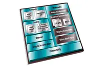 Texas Instruments has launched what it says is the most powerful embedded SoCs. The Sitara AM57x range also offers real time processing and a range of multimedia features.
Adrian Valenzuela, marketing director, noted: “We haven’t seen anything like this in the market. It’s a combination of heterogeneous cores, including Cortex-A15, TMS320C66x and Cortex-M4, that has beed designed to support a broad range of customers, but which is also easy to use.”
Five devices have been announced, all manufactured on a 28nm ultra low power process. The AM5726 and 5728 have dual A15 cores and dual C66x DSPs, while the AM5716 and 5718 have single A15 and C66x cores. The A15 cores run at 1.5GHz, while the C66x DSPs are clocked at 750MHz. The fifth part features one A15 core and one C66x, with both cores running at 500MHz.
The A15 and DSP cores are intended for compute applications, while the twin Cortex-M4 cores are paired with a quad core programmable real time unit – or PRU – to handle control operations. Valenzuela noted the control cores ensure deterministic real time processing and low latency I/O.
“The dual A15 and dual DSP cores can handle applications that need a lot of horsepower,” he noted, “while the M4/PRU combination means good latency. And the AM57x is the only general purpose family that can run industrial communications protocols on the processor.”
TI has worked with the Beagleboard organisation to create the BeagleBoard-X15. The device, which features the AM5728 SoC, is likely to retail for around $199 and is expected to ship in the latter part of 2015. Also available is the TMDXEVM5728 evaluation module. The X15 based device adds a 7in capacitive touchscreen and a 3Mpixel camera.
Developers will be able to take advantage of a single SDK for all parts in the range. This will bring the mainline 2015 LTS Linux Kernel 4.1, as well as TI-RTOS and the Linaro tool chain.
Asked whether TI is looking to add ARM v8 based devices to the range, Valenzuela noted that, while there maybe a place for them, there remains a large part of the market which values the Cortex-A15.
Author
Graham Pitcher
Source: www.newelectronics.co.uk
 ThingWorx has announced it is working with Analog Devices to offer customers an integrated sensor to cloud environment using the ThingWorx IoT Platform.
Russell Fadel, president of ThingWorx, said: “We’re excited to collaborate with Analog Devices and endeavor to solve IoT infrastructure challenges such as connectivity, communications and other foundational services, so that customers can focus their time and energy on creating IoT applications to generate business value.”
The collaboration is designed to make it easier for customers to bridge the physical and digital worlds with technologies that sense, measure and connect.It will support the IoT journey of smart, connected product data from devices and sensors to wireless communication to big data collection and analysis.
“Our vision in this IoT era is to help companies harness the power of the data generated from sensors in smart, connected products,” said Martin Cotter, vice president, Healthcare, Consumer and IoT, Analog Devices. “Through our collaboration with ThingWorx, we will strive to enhance our customers’ experience utilising the data provided to the ThingWorx IoT Platform to empower rapid, rich and interactive IoT applications, real-time dashboards, collaborative workspaces, and mobile interfaces quicker than ever before.”
Pic: Russell Fadel, president of ThingWorx
Author
Tom Austin-Morgan
Source: www.newelectronics.co.uk
 Apple may have to pay a substantial settlement to the University of Wisconsin after a US federal jury found the company guilty of infringing a University patent – US Patent 5781752 – that helps to improve processor efficiency.
The suit was filed by the Wisconsin Alumni Research Foundation (WARF), which commercialises research at the University. It alleged that Apple used its technology in its A7, A8 and A8X processors, which feature in some iPhones and iPads.
It’s not the first time that WARF has taken on the electronics industry; the commercialisation body sued Intel in 2008, alleging infringement of the same patent. However, the case was settled out of court before the trial began.
In the latest case, US District Judge William Conley is assessing three aspects: liability; damages; and whether Apple infringed the patent ‘willfully’. In its suit, WARF has asked for more than $860million in damages.
WARF has also filed another suit which cites illegal use of the patent by Apple in the A9 and A9X processors found in the iPhone 6S and 6S Plus, as well as the iPad Pro.
The abstract of the University of Wisconsin patent – filed in December 1996 and published in July 1998 – states: ‘A predictor circuit permits advanced execution of instructions depending for their data on previous instructions by predicting such dependencies based on previous mis-speculations detected at the final stages of processing. Synchronization of dependent instructions is provided by a table creating entries for each instance of potential dependency. Table entries are created and deleted dynamically to limit total memory requirements’.
Apple has referenced US Patent 5781752 in several of its patents.
Author
Graham Pitcher
Source: www.newelectronics.co.uk
 According to a report by Beecham Research, it is expected that Low Power Wide Area Networks (LPWANs) will provide 26% of the total IoT connectivity market by 2020 with 345million connections, marking an end to the near monopoly of traditional cellular networks for machine connectivity.
“LPWANs represent the most dynamic and potentially game changing development in the M2M/IoT market,” said David Parker, senior analyst at Beecham Research and the author of the report. “The lower speeds of LPWANs are the trade-off for longer range, offering networks optimised for machine connectivity with much lower deployment costs than traditional cellular networks. LPWANs will both compete and collaborate with cellular and other network technologies to stimulate market growth with more connectivity options for end-users. “
The Beecham Research report investigates the increasing plethora of LPWAN technologies including the likes of Sigfox and companies in the LoRa Alliance, which are currently leading the LPWAN field in terms of network deployment, industry support, investment and customers. Most of these LPWAN solutions use the ISM (Industrial Scientific and Medical) bands better known for use by short range wireless technologies like Zigbee, Wifi and 6LoWPAN. However, recent advances have enabled LPWANs to be established using the ISM bands over longer distances, up to 50km in rural areas and 5 to 10km in urban areas.
Another LPWAN technology with long range, low power characteristics is known as TV White Spaces (TVWS), which uses the gaps in between VHF/UHF parts of the spectrum, previously used for TV broadcasting. TVWS promises connectivity over distances of 10km and with superior in-building penetration when compared to 3G or 4G.
“New entrants working in the ISM and TVWS bands are promoting overall market growth and providing a spur to action within the GSMA world,” said Parker. “Developing standards for the cellular operating community is a slower process but the emergence of LTE-M and Narrowband IoT (NB-IOT) will allow cellular operators to compete with these new entrants on a level playing field of range, battery life and costs.”
Pic: David Parker, senior analyst at Beecham Research
Author
Tom Austin-Morgan
Source: www.newelectronics.co.uk