
Electronics News
Archive : 17 October 2015 год
 Loughborough University has been awarded £3.9million to develop a new way of designing and fabricating high frequency communications circuitry. The funding from the EPSRC will be used to establish the SYMETA – SYnthesizing 3D METAmaterials for RF, microwave and THz applications – research programme.
Current conventional printed circuit board manufacturing and assembly processes involve harsh chemicals, etching, high volumes of water and high temperatures. SYMETA’s aim is to employ metamaterial technology to construct the circuits and reduce both the number of processes involved in the circuit manufacture and the components soldered onto the boards.
Metamaterials are engineered composite materials that have certain electromagnetic properties not normally found in nature, and can therefore be designed to create high frequency circuitry like that found in mobile phones
Industries that could benefit from the research include aviation, space, healthcare and the military.Employing the advanced manufacturing techniques that the consortium will develop will also remove the need for the harsh chemicals typically used in the manufacture of traditional circuit boards, offering significant environmental benefits.
The SYMETA team will be led by Professor Yiannis Vardaxoglou from Loughborough University. The other research partners include the Universities of Exeter, Oxford, Sheffield and Queen Mary, University of London.
Prof Vardaxoglou said: “Introducing these novel structures into the complex world of electronic design will offer a radical new way of designing and manufacturing electronics at low cost. We are grateful to EPSRC for supporting such an innovative and timely project.”
The funding for SYMETA was announced by Science Minister Jo Johnson, as part of a £21m investment by the EPSRC into research that aims to tackle some of the major challenges facing science and engineering.
Pic: Professor Yiannis Vardaxoglou, Loughborough University
Author
Tom Austin-Morgan
Source: www.newelectronics.co.uk
 Seven research programmes that aim to tackle some of the UK’s major science and engineering challenges were given the green light today by the Universities and Science Minister, Jo Johnson.
Academics, industrialists and policy makers will address issues such as: how new ways of using robotics and autonomous systems can restore the balance between engineered and natural systems in the cities of the future; how to understand the nature of meta-materials and advanced materials for use in electronic systems and the manufacture of new devices; and how to understand the complexity and interconnectedness of systems, identify critical and vulnerable dependencies, prevent their failure and improve their resilience and reliability.
The research consortia will involve nineteen UK universities and eighty partners with £21million of funding secured by the EPSRC. They will begin work in December and are supported by an additional £11m investment from industry, bring the total level of support to £32m.
Universities and Science Minister Jo Johnson said: “As a One Nation Government we are investing in world-class science and engineering across our country. We want the UK to be the best place in Europe to innovate and this £21m investment will bring together the nation’s researchers to address some of the most pressing engineering challenges we face. From ground-breaking work with robotics to advanced air-flow simulators, this investment will help tackle our aging water infrastructure and air pollution in cities to improve the lives of millions of people around the world.”
Pic: Universities and Science Minister Jo Johnson
Author
Tom Austin-Morgan
Source: www.newelectronics.co.uk
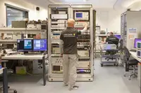 Yokogawa’s European Calibration Laboratory, based at the company’s European Headquarters in Amersfoort, Netherlands, has become the world’s first non-governmental facility to receive full ISO17025 Accreditation for power measurements at up to 100kHz. This is in addition to its capability for providing high-accuracy calibration at 50Hz.
There is a growing demand to remove uncertainty in power measurements, particularly with the growing focus on renewable energy markets and the need to optimise energy efficiency while complying with international standards on power quality, especially at low power factors. In addition, the inverters used in renewable energy systems are switching at higher speeds: a scenario that introduces harmonics at higher frequencies.
There is also a demand for high-frequency power measurements on devices such as switch-mode power supplies, electronic lighting ballasts, soft starters in motor controls and frequency converters in traction applications. As a result, power calibration at 50Hz is no longer sufficient, and accredited power calibration at up to 100kHz is necessary to address these markets.
Terry Marrinan, Yokogawa’s vice president of test and measurement said: “The recognition offered by ISO17025 accreditation is objective proof that the knowledge of our personnel and the quality of our instruments are at a world-class level.”
The Calibration Laboratory’s accreditation will provide Yokogawa with an essential development tool for the future, ensuring that new products will have undergone the most rigorous compliance testing and certification before release. Yokogawa’s customers can also be confident that they have access to accredited traceable power calibration for all their needs, avoiding time-consuming submission to national standards laboratories.
In addition to wideband and accurate power-meter calibration systems, the calibration laboratory also includes systems for calibrating oscilloscopes, recorders and optical products, and is therefore capable of calibrating a wide range of instruments in the test and measurement industry.
Author
Tom Austin-Morgan
Source: www.newelectronics.co.uk
 Researchers from the University of Missouri are on the path to creating biodegradable electronics by using organic components in screen displays. The researchers' advancements could one day help reduce electronic waste in landfills.
On average, consumers replace their mobile phones every 22 months, throwing away more than 150 million phones a year in the process. When it comes to recycling and processing all of this electronic waste, the World Health Organisation reports that even low exposure to the electronic elements can cause significant health risks.
"Current mobile phones and electronics are not biodegradable and create significant waste when they're disposed," said Suchismita Guha, professor in the Department of Physics and Astronomy at the MU College of Arts and Science. "This discovery creates the first biodegradable active layer in organic electronics, meaning, in principle, we can eventually achieve full biodegradability."
Guha, along with graduate student Soma Khanra, collaborated with a team from the Federal University of ABC (UFABC) in Brazil to develop organic structures that could be used to light handheld device screens. Using peptides, or proteins, the researchers were able to demonstrate that these tiny structures, when combined with a blue light-emitting polymer, could successfully be used in displays.
"Peptides can self-assemble into beautiful nanostructures or nanotubes, and, for us, the main goal has been to use these nanotubes as templates for other materials," Guha said. "By combining organic semiconductors with nanomaterials, we were able to create the blue light needed for a display. However, in order to make a workable screen for your mobile phone or other displays, we'll need to show similar success with red and green light-emitting polymers."
The scientists also discovered that by using peptide nanostructures they were able to use less of the polymer. Using less to create the same blue light means that the nanocomposites achieve almost 85% biodegradability.
"By using peptide nanostructures, which are 100% biodegradable, to create the template for the active layer for the polymers, we are able to understand how electronics themselves can be more biodegradable," Guha said. "This research is the first step and the first demonstration of using such biology to improve electronics.”
Pic: The illustration shows a theoretical simulation of the distribution of the polymer on peptide nanotubes and an electron microscopy image of the nanocomposite
Author
Tom Austin-Morgan
Source: www.newelectronics.co.uk
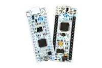 STMicroelectronics is extending its range of STM32 Nucleo development boards with scalable, small-form-factor variants to support the 32-pin members of its STM32 microcontroller family. The STM32 Nucleo-32 boards come with direct support from a choice of IDEs and direct access to mbed online resources. The STM32 Nucleo open platform is said to enable affordable prototyping using STM32 MCUs combined with a range of hardware plug-ins through Arduino Nano connectors.
Developers can also take full advantage of the STM32 software libraries as well as STM32Cube tools to facilitate software development and port designs from one STM32 variant to another. The STM32 Nucleo boards include the ST-LINK debugger/programmer, which enables drag-and-drop flash programming, so there is no need for a separate debug probe. Since the STM32 Nucleo boards are mbed-enabled, developers can make use of the mbed online tools and collaboration infrastructure at the mbed website.
Makers and engineers can choose between three versions of the STM32 Nucleo-32 boards based on the STM32F031, STM32F042, and STM32F303. In addition, STM32L0 and STM32L4 ultra-low-power series will be supported early in 2016.
Author
Tom Austin-Morgan
Source: www.newelectronics.co.uk
 Bosch has opened a €310million research campus at Rennigen, on the outskirts of Stuttgart, to encourage interdisciplinary collaboration and innovation.
Dr Volkmar Denner, chairman of the Bosch board of management, said: “Like a university, our campus brings together many faculties. Here, we want our researchers to do more than just think about what the future could bring. We want them to be successful entrepreneurs as well. Renningen is Bosch’s own Stanford.”
The campus will employ 1700 engineers performing applied industrial research in the fields of electrical engineering, mechanical engineering, computer science, analytics, chemistry, physics, biology, or microsystems technology. Their work will focus on areas such as software engineering, sensor technology, automation, driver assistance systems, and battery technology, as well as on improved automotive powertrain systems.
Author
Tom Austin-Morgan
Source: www.newelectronics.co.uk