
Electronics News
Archive : 2 March 2016 год
 Europe’s technology leaders in the development of flexible organic light-emitting diodes (OLEDs) for lighting and signage applications have formed a consortium, called ‘PI-SCALE’, that aims to create a Europe-wide pilot line to enable companies of all sizes to quickly and cost effectively test and scale up their flexible OLED lighting concepts and turn them into market ready products. The project is supported by the European Commission through the Photonics Public Private Partnership with a contribution of €14million.
Flexible OLEDs have the potential to be integrated into formed parts or bonded onto curved surfaces, the commercialisation of this technology is claimed to open up a host of design opportunities to create value adding lighting products in application areas such as architecture, automotive, aerospace and consumer electronics.
PI-SCALE will offer capability and services in the pilot production of customised flexible OLEDs and initially focuses on product streams in the areas of automotive, designer luminaires and aeronautics.
The project will allow companies to test and develop their applications at an industrial scale, achieving the product performance, cost, yield, efficiency and safety requirements that facilitate mass market adoption. The consortium will combine and utilise existing capability from each of the partners to create a self-standing, open access European flexible OLED pilot line. It is said the pilot line will be available during and after the lifetime of the project to companies on an open access basis.
Dr Joanne Wilson from the Holst Centre, the coordinators of the project, said: “The creation of this pilot line is a fantastic opportunity for companies to get flexible OLED technology out of the research and development phase and into products.”
PI-SCALE is one of three major pilot lines which have been launched by the European Photonics Public Private Partnership to help companies take photonics technologies from the lab into commercial markets. The two other pilot lines ‘MIRPHAB’ and ‘PIX4Life’ will focus on photonics technologies for health applications and sensors for the detection of chemicals in gas and liquids.
Author
Tom Austin-Morgan
Source: www.newelectronics.co.uk
 A team of researchers, led by a group from the University of California, Riverside, claims to have demonstrated the first transmission of electrical signals through insulators in a sandwich-like structure, a development that could help create more energy efficient electronic devices.
The UC Riverside-led research is said to be significant because it demonstrates that a tri-layer, sandwich-like, structure can serves as a scalable pure spin current device, an essential ingredient in spintronics.
A key element in this breakthrough is the material. To demonstrate the effect, the magnetic insulator needs to be truly insulating, or there will be a parasitic signal from leakage. On the other hand, a high-quality magnetic insulator grown on metal had never been demonstrated.
Jing Shi, professor of physics at the University of California, Riverside, said: "Using a combination of sputtering and pulsed laser deposition, we showed that the 50 to 100nm thick magnetic insulator, in this case yttrium iron garnet, is not only magnetic and insulating, but also of high quality when it is grown on 5nm thick platinum."
In the structures used by the researchers, there are two metals and a magnetic insulator in between. The metals are for spin current generation and detection via the spin Hall effect and inverse spin Hall effect.
The magnetic insulator is an electrical insulator but a good spin current conductor. The spin current flowing in the insulator does not involve mobile electrons therefore it does not dissipate energy as an electrical current does in joule heating.
The researchers also claim to have demonstrated that the signal transmission can be switched on and off and modulated in its strength by a magnetic field. The electrical signal transmission through the magnetic insulators can be switched on and off depending on the magnetic state, or direction of the magnetisation, of the magnetic insulators.
This means that the direction of the magnetisation can be regarded as a memory state of non-volatile random access memory devices. In addition, the signal level can be modulated by changing the direction of the magnetisation; suiting it for use in analogue devices. The researchers also say that sandwich structure can be scaled down with nanofabrication.
Pic: Jing Shi, professor of physics at the University of California, Riverside
Author
Tom Austin-Morgan
Source: www.newelectronics.co.uk
 Keysight Technologies has announced turn-on chipsets using indium phosphide (InP) semiconductor technology that it says will bring real-time and equivalent-time oscilloscopes offering bandwidths greater than 100GHz.
The company says the oscilloscopes will also feature 10-bit A/D converters and more than one maximum bandwidth input channel per oscilloscope.
Likely applications for these high bandwidth oscilloscopes include 5G mobile systems with the upcoming IEEE P802.3bs 400G, as well as terabit coherent optical modulation, which will need oscilloscopes for electrical parametric measurements.
Keysight claims it is the only company that produces oscilloscopes made with InP chipsets. Investing in the InP process is said to have allowed the company to scale the transistor switching frequencies beyond the 300GHz level, enabling higher bandwidths in both the chips and the end products.
“Our goal is to move multiple performance parameters ahead simultaneously,” said Dave Cipriani, vice president and general manager of Keysight’s oscilloscope business “The next-generation oscilloscopes deliver bandwidths starting at 80GHz and going beyond 100GHz. They will have a lower noise density, providing higher-resolution measurements in tightly-synchronised, multi-channel systems. Whether customers are measuring higher baud rates, higher order QAM signals or multi-channel systems, these next-generation scopes will meet their needs.”
This announcement coincides with the start of Keysight’s Scope Month, during which it will offer oscilloscope measurement tips and content, access to measurement experts and daily oscilloscope giveaways.
Pic: Shown here is the Keysight high-performance oscilloscope acquisition system
Author
Tom Austin-Morgan
Source: www.newelectronics.co.uk
 SmartKem has reported its solution-processed organic semiconductor, tru-FLEX, has set a world record in digital circuit performance. The tru-FLEX-based five-stage organic thin-film transistor (OTFT) ring oscillator using solution coating is claimed to operate with an oscillation frequency above 500kHz and stage delay of less than 200ns.
This is said to be the highest frequency reported to date for a unipolar ring oscillator fabricated using a solution-processed organic semiconductor and gate dielectric. It is also expected that with minor optimisation of the circuit design, oscillator frequencies above 1MHz could be attained.
Integrated circuits based on OTFTs have been in development for over 15 years with development scientists working on both the speed and complexity of integrated circuits for a range of electronics applications. However, one of the main barriers to the growth of printed electronic circuits was the ability to manufacture circuits using high-throughput, solution-coating techniques with the necessary semiconductor performance to allow fast logic circuits to be realised in standard digital circuits such as ring oscillators.
This result demonstrates that this historic barrier no longer exists, opening the door to a range of application possibilities. For instance, with the emergence of the Internet of Things, one market requirement that has not been met is for low-cost, thin, flexible and disposable RFID and NFC tags for the transmission of data from devices, sensors or objects. To achieve the necessary bit rate of 53kbits/s for a RFID or NFC device operating at the standardised frequency of 13.6MHz, a stage gate delay in the logic of less than 400ns is needed: Two times slower than SmartKem’s ring oscillator.
A more immediate application is as a TFT backplane platform for the manufacture of conformal LCD and flexible AMOLED displays. SmartKem says narrow bezels can now be achieved by the use of ‘integrated gate drivers’ fabricated on the display backplane. Whilst it was once thought that this could only be achieved using inorganic materials such as LTPS, this result shows that tru-FLEX would allow the manufacture of integrated gate drivers that would not only drive 4K2K displays, but would also offer true physical flexibility.
Author
Tom Austin-Morgan
Source: www.newelectronics.co.uk
 Finland's VTT Technical Research Centre and Aalto University, together with a number of partners, are embarking on a project to develop optical switching and transmission technologies. The work is intended to improve the scalability and energy efficiency of data centres and 5G networks.
The project, part of Finnish funding agency Tekes’ 5thGear programme, is called Optical Information Processing for Energy Efficient Data Centres (OPEC). It will focus on the development of novel optical components and technologies based on VTT’s proprietary silicon photonics platform, as well as on new silicon wafer production and precision assembly concepts. The project, supported by Nokia, Rockley Photonics, Okmetic, nLight, Ginolis and Picosun.
The partners are looking to develop active photonic components based on graphene and other layered 2D materials in order to achieve levels of performance beyond the theoretical limit of the traditional materials. The project also explores the feasibility of integrated photonics in analogue signal transfer and manipulation, such as radio over fibre and microwave beam steering in mobile link stations.
Author
Graham Pitcher
Source: www.newelectronics.co.uk
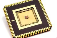 Nanoelectronics research centre imec and Holst Centre have developed an ECG readout chip which uses time domain circuit techniques. According to the partners, the device offers consistent beat detection abilities and may pave the way for low cost, low power multisensor SoCs for wearable medical devices.
The chip, which has an area of 0.015mm2, is implemented in 40nm TSMC CMOS process. Consuming 3.3µW from a 0.6V supply, the device is said to handle an AC sigma of up to 40mVpp and DC electrode offset of up to 300mV.
Constant beat detection is supported by the ECG signal being acquired from the noise-stress database, meaning the system does not saturate. The time domain based readout architecture, said to take advantage of technology scaling, avoids the need for analogue circuitry. In imec’s opinion, current analogue circuit techniques don’t scale well enough and analogue front end readout chips face significant challenges in combining a large dynamic range with small size and low power consumption.
“Our breakthrough readout ECG chip paves the way to low cost, low power multisensory systems for ambulatory medical applications,” said Nick Van Helleputte, team leader biomedical circuits at imec. “Furthermore, it opens innovation paths for analogue front end design beyond 40nm, leveraging the power and area benefits of scaled technology in digital architectures.”
Author
Graham Pitcher
Source: www.newelectronics.co.uk