
Electronics News
Archive : 7 March 2016 год
 In a development which has potentially wide ranging implications, a UK research team says it has demonstrated the first practical laser that has been grown directly on a silicon substrate.
As data rates continue to climb, passing data between chips using conventional electrical interconnects is proving more and more difficult. The solution is to use light, rather than copper, but it has proved troublesome to integrate this functionality directly onto silicon.
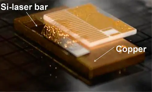
Now, an EPSRC funded group led by Cardiff University and including researchers from UCL and the University of Sheffield, says it has solved the problem and has grown a laser directly onto a silicon substrate. Professor Huiyun Liu, who led the growth activity, said the 1300nm wavelength laser has been shown to operate at temperatures of up to 120°C and for up to 100,000 hours.
Professor Peter Smowton, from Cardiff’s School of Physics and Astronomy, said: “Realising electrically pumped lasers based on silicon substrates is a fundamental step towards silicon photonics.
“The precise outcomes of such a step are impossible to predict in their entirety, but it will clearly transform computing and the digital economy, revolutionise healthcare through patient monitoring and provide a step-change in energy efficiency.
“Our breakthrough is perfectly timed as it forms the basis of one of the major strands of activity in Cardiff University’s Institute for Compound Semiconductors and the University’s joint venture with compound semiconductor specialist IQE.”
Professor Alwyn Seeds, head of the Photonics Group at University College London, added: “The techniques that we have developed permit us to realise the Holy Grail of silicon photonics – an efficient and reliable electrically driven semiconductor laser integrated directly on a silicon substrate. Our future work will be aimed at integrating these lasers with waveguides and drive electronics, leading to a comprehensive technology for the integration of photonics with silicon electronics."
Author
Graham Pitcher
Source: www.newelectronics.co.uk
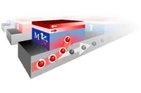 MRAM (magnetic random access memory) is faster, more efficient and robust than other kinds of data storage. However, switching bits still requires too much electrical power to make large-scale application practicable. Researchers at Eindhoven University of Technology (TU/e) say they have discovered a way of solving this problem by using a 'bending current'.
MRAM stores data by making use of the 'spin' of electrons. Since magnetism is used instead of an electrical charge, the memory is permanent – even when there is a power failure. These magnetic memories also use less power, which means that battery life can be extended in mobile phones, for example.
In MRAM bits are projected by the direction of the spin of the electrons in a piece of magnetic material: for example, upwards for a '1' and downwards for a '0'. The storage of data occurs by flipping the spin of the electrons over to the correct side. Normal practice is to send an electrical current which contains electrons with the required spin direction through the bit. The large quantity of electrical current needed to do this has hindered a definitive breakthrough for MRAM.
The TU/e physicists’ method is claimed to flip the magnetic bits faster and more energy-efficiently. A current pulse is sent under the bit, which bends the electrons at the correct spin upwards through the bit. "It's a bit like a soccer ball that is kicked with a curve when the right effect is applied," explained Arno van den Brink, TU/e PhD student.
This method is said to be fast, but needs something more to make it reliable. Earlier attempts required a magnetic field, but that made the method expensive and inefficient. The TU/e researchers claim to have solved this by applying an anti-ferromagnetic material to the top of the bits. This is said to enable the requisite magnetic field to be frozen, as it were, making the process more energy-efficient and lowering cost. "This could be the decisive nudge in the right direction for superfast MRAM in the near future," said Van den Brink.
Pic: A magnetic bit is being switched by bending electrons with the correct spin upwards through the bit. A special anti-ferromagnetic material on top of the bits is claimed to make the process reliable
Author
Tom Austin-Morgan
Source: www.newelectronics.co.uk