
Electronics News
Archive : 2 April 2016 год
 PTC has announced its Vuforia augmented reality (AR) platform will support Microsoft HoloLens. This capability has been demonstrated at Build 2016, Microsoft’s annual developer conference at San Francisco.
Vuforia allows the HoloLens to connect experiences to specific things in the environment. This capability has been used to create 3D visualisations of various consumer and industrial products. When combined with HoloLens, these 3D visualisations can be expanded and transported to actual size in any environment, providing a more immersive and realistic visualisation experience.
The system can also be used to create guided step-by-step instructions for technicians on products or machinery to help reduce or eliminate dependence on physical manuals.
Jeff Lind, eBusiness Innovation at Caterpillar, said: “AR could help provide hands-free, voice access to visual information as a customer configures a product solution or performs maintenance and repair procedures on the equipment.”
With Vuforia, developers can build a universal Windows platform application that can run on Windows 10 devices such as phones, tablets, VR viewers, and digital eyewear, enabling them to target the broadest range of devices with reliable AR experiences, whether for consumer or enterprise-facing applications.
“We are excited about Microsoft’s vision for Windows 10 and HoloLens,” said Jay Wright, senior vice president and general manager, Vuforia, PTC. “We share this vision, and look forward to enabling new experiences on Windows 10 tablets and HoloLens that will fundamentally change the way we work.”
The Vuforia SDK is expected to be available spring 2016.
Author
Tom Austin-Morgan
Source: www.newelectronics.co.uk
 The Centre for Process Innovation (CPI) is leading a consortium to create a UK manufacturing supply chain that aims to enable the widespread adoption of packaging incorporating Near-field Communication (NFC) based technology.
The three year project, entitled ‘SCOPE’, is building the manufacturing capability, capacity and skills required to commercialise and position the UK as a world leader in the production of smart products with printed sensors – a fast growing billion dollar global market.
The aim of SCOPE is to develop processes, equipment and applications to enable the high-volume manufacturing of printed electronic components that incorporate NFC. The project is providing a technology platform to develop innovative and novel functionalities and applications, alongside the building of specialist skills and capabilities. A key emphasis is to apply highly automated and high speed integration techniques to meet target costs of <1cent per NFC tag.
The consortium is made up of 14 partners across the UK’s packaging supply chain including; Unilever, Hasbro, Crown Packaging alongside Tier-1 product supply-chain companies Andrews & Wykeham and Mercian Labels. Additionally it unites complementary technical expertise in the production of flexible integrated circuits (PragmatIC), the automation of processes (Optek), ferrite materials (University of Kent), electronics design (Silvaco), polymer substrates (Innovia), inks (Invotec and CPI), NFC know-how (NFS) and systems integration (CPI and PragmatIC). The British Print Industry Federation are supporting dissemination for the project, linking the supply chain together and providing end user feedback on the market readiness of the technology.
The project covers multiple application sectors such as fast-moving consumer goods, beverage, games and security and provides a platform to develop second-generation opportunities within other key UK sectors including healthcare, food, energy, built-environment, defence and transport.
Mike Clausen programme manager at CPI said: “Going forward the next steps are to upscale the manufacturing process to ensure that these novel NFC applications are produced at the cost and speeds that industry demands. To do this, we are currently developing the capability to scale up these production processes to produce market trial samples of 50,000 to 100,000 tags”.
Author
Tom Austin-Morgan
Source: www.newelectronics.co.uk
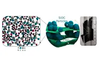 A team of researchers from Kansas State University, led by Gurpreet Singh, associate professor of mechanical and nuclear engineering, has created a paperlike battery electrode using silicon oxycarbide-glass and graphene.
The battery electrode is claimed to be more than 10% lighter than other battery electrodes and has close to 100% cycling efficiency for more than 1000 charge discharge cycles. It is made of low-cost materials that are byproducts of the silicone industry. And it functions at temperatures as low as -15°C, which suits it to numerous aerial and space applications.
Prof Singh said: "The paperlike design is markedly different from the electrodes used in present day batteries because it eliminates the metal foil support and polymeric glue -- both of which do not contribute toward capacity of the battery."
Until now, it has been difficult to incorporate graphene and silicon into practical batteries because of challenges that arise at high mass loadings, such as low capacity per volume, poor cycling efficiency and chemical-mechanical instability.
Prof Singh's team has addressed these challenges by manufacturing a self-supporting electrode consisting of a glassy ceramic called silicon oxycarbide sandwiched between large platelets of chemically modified graphene. The electrode is said to have a capacity of approximately 600mA-hours per gram.
The silicon oxycarbide material is prepared by heating a liquid resin to the point where it decomposes and transforms into sharp glasslike particles. The silicon, carbon and oxygen atoms get rearranged into random 3D structure and any excess carbon precipitates out into cellular regions. Its open 3D structure creates large sites for reversible lithium storage and smooth channels for lithium-ion transportation. This structure and mechanism of lithium storage is different than crystalline silicon electrodes. Silicon oxycarbide electrodes are expected to be low cost because the raw material (liquid resin) is a byproduct of the silicone industry.
Moving forward, Prof Singh and his team want to address practical challenges. Singh's goal is to produce this electrode material at larger dimensions. For example, present-day pencil-cell batteries use graphite-coated copper foil electrodes that are more than one foot in length. The team also wants to perform mechanical bending tests to see how they affect performance parameters.
"Ultimately, we would like to work with industry to explore production of lithium-ion battery full-cells," Prof Singh said. "Silicon oxycarbide can also be prepared by 3D printing, which is another area of interest to us."
Author
Tom Austin-Morgan
Source: www.newelectronics.co.uk
 According to research by Japanese startup, Flosfia, gallium oxide could replace silicon as the best material for use in electronic components such as diodes and transistors as it is cheaper, more efficient and capable of handling high voltages.
Although this weakness is addressed by devices made from silicon carbide and gallium nitride, both have had limited commercial success due to high prices. Flosfia claims that its gallium oxide diodes are already performing more efficiently than those made from SiC and GaN.
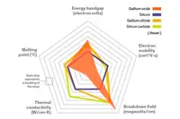
The superiority of these gallium oxide devices stems from the material’s approximately 5eV bandgap-higher than that of gallium nitride (about 3.4 eV) or silicon carbide (about 3.3 eV). A bigger bandgap enables a material to withstand a stronger electric field, making it possible to use a thinner device for a given voltage. The thinner the device, the lower its resistance, and thus the more efficient it is.
Gallium oxide devices do not excel in all areas. Their Achilles’ heel is poor thermal conductivity. Flosfia’s engineers have improved the device architecture to address that very issue. In particular, they found a way to make the diode chip thinner, according to Naonori Kurokawa, a partner at University of Tokyo Edge Capital, a Flosfia investor. The key is to grow the gallium oxide crystal on a sapphire substrate.
The process Flosfia uses for making gallium oxide devices was invented by company cofounder and Kyoto University professor Shozuo Fujita. In it, the sapphire substrate is heated and a fine mist of particles is transferred into the chamber via a nonreactive ‘carrier gas’. The mist, which contains metal compounds, decomposes when it hits the hot substrate and forms a film of gallium oxide. The whole process can be cycled through rapidly because, unlike with other methods, the chamber never has to be completely evacuated, driving down costs.
The Flosfia engineers found that their device combines a 531V breakdown voltage with an on-resistance of 0.1mO/cm2, exceeding the limits of what is possible with silicon carbide.
Kurokawa explains that the diodes have modest breakdown voltages because they are bare chips. Introducing insulating layers into this very simple device should lead to significant improvement, he said.
Flosfia aims to provide samples of its diodes to potential customers later in 2016 with a ramp-up of diode production in 2018 and the development and launch of accompanying transistors.
Pic: Flosfia’s gallium oxide devices exploit the material’s big bandgap and breakdown field while making up for its poor thermal conductivity. (Values are normalised to silicon’s [blue].)
Author
Tom Austin-Morgan
Source: www.newelectronics.co.uk