
Electronics News
Archive : 11 April 2016 год
 Research scientists at the Leibniz Institute for New Materials (INM) have developed a single stage process that allows conductive paths just a few microns wide to be created on carrier materials such as glass and flexible foils. Previously, says the team, manufacturing conductive paths was a time consuming process using several steps. The team believes its work could enable the development of appliances with flexible or rollable touchscreens.
The process is based on photochemical metallisation of silver compounds. Several methods are said to be available to transfer these silver compounds on to plastic foil or glass, with paths as small as 1µm. By irradiating these with UV light, the silver compounds are transformed into electrically conductive metallic silver. This basic principle allows conductive paths to be created individually.
“There are three possibilities,” said Peter William de Oliveira, head of optical materials, “depending on the requirements. Writing conductive paths using UV lasers is particularly suitable for initial prototype manufacture and testing the design. However, for mass production, this method is too time consuming.”
Photomasks can also be used for structuring. “For a semi continuous process,” he continued, “these are particularly suitable for applying the conductive paths on glass.”
The researchers are currently developing the third method, which uses transparent stamps. “These stamps push out the silver compound mechanically; conductive paths then only occur where there is still silver compound,” de Oliveira explained. Since the stamps are made of soft plastic, they can be arranged on a roll and INM researchers are now working on embedding the UV source directly.
Author
Graham Pitcher
Source: www.newelectronics.co.uk
 Harnessing solar power is said by researchers to require a material that not only absorbs light efficiently, but which also converts the energy to highly mobile electrical current. Looking to find this ‘ideal mix’ in a single material is a challenge, so scientists have been experimenting with ways to ‘hybrids’.
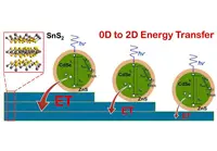
Scientists from the US Brookhaven National Laboratory, Stony Brook University and the University of Nebraska have combined the light harvesting properties of quantum dots with the tunable electrical conductivity of a layered tin disulphide semiconductor. The work is said to pave the way for the use of these materials in a range of optoelectronic applications.
According to Brookhaven chemist Mircea Cotlet: “Two dimensional metal dichalcogenides, like tin disulphide, have some promising properties for solar energy conversion and photodetector applications, including a high surface to volume aspect ratio. But no semiconducting material has it all. These materials are very thin and are poor light absorbers. So we were trying to mix them with other nanomaterials, like light absorbing quantum dots, to improve their performance through energy transfer.”
The researchers found the rate for non radiative energy transfer from individual quantum dots to tin disulphide increased with the number of tin disulphide layers. Looking to test their work, the team incorporated the hybrid material into a photo FET. According to the results, the hybrid material enhanced the performance of the photo FETs dramatically, with a photocurrent response 500% better than FETs made with tin disulphide alone.
Cotlet concluded: “The idea of ‘doping’ 2D layered materials with quantum dots to enhance their light absorbing properties shows promise for designing better solar cells and photodetectors.”
Author
Graham Pitcher
Source: www.newelectronics.co.uk
![]() Engineers from the University of Pennsylvania claim to have developed an approach for making transistors by sequentially depositing their components in the form of liquid nanocrystal ‘inks’.
Engineers from the University of Pennsylvania claim to have developed an approach for making transistors by sequentially depositing their components in the form of liquid nanocrystal ‘inks’.
The researchers began by taking nanocrystals, or roughly spherical nanoscale particles, with the electrical qualities necessary for a transistor and dispersing these particles in a liquid, making nanocrystal inks: a conductor (silver), an insulator (aluminium oxide), a semiconductor (cadmium selenide) and a conductor combined with a dopant (a mixture of silver and indium).
"These materials are colloids just like the ink in your inkjet printer," Cherie Kagan, Professor in the School of Engineering and Applied Science, said. "But you can get all the characteristics that you want and expect from the analogous bulk materials, such as whether they're conductors, semiconductors or insulators. Our question was whether you could lay them down on a surface in such a way that they work together to form functional transistors."
The electrical properties of several of these nanocrystal inks had been independently verified, but the researched say that they had never been combined into full devices. Such a process entails layering or mixing them in precise patterns.
First, the conductive silver nanocrystal ink was deposited from liquid on a flexible plastic surface that was treated with a photolithographic mask then rapidly spun to draw it out in an even layer. The mask was then removed, leaving the silver ink in the shape of the transistor's gate electrode. The researchers followed that layer by spin-coating a layer of the aluminium oxide nanocrystal-based insulator, then a layer of the cadmium selenide nanocrystal-based semiconductor and finally another masked layer for the indium/silver mixture, which forms the transistor's source and drain electrodes. Upon heating at low temperatures, the indium dopant diffused from those electrodes into the semiconductor component.
"The trick with working with solution-based materials is making sure that, when you add the second layer, it doesn't wash off the first, and so on," Prof Kagan said. "We had to treat the surfaces of the nanocrystals, when they're first in solution and after they're deposited, to make sure they have the right electrical properties and that they stick together in the configuration we want."
The researchers claim they were able to make several transistors on the same flexible plastic backing at the same time because this entirely ink-based fabrication process works at lower temperatures than existing vacuum-based methods. Prof Kagen added that these nanocrystal-based field effect transistors could eventually be constructed by additive manufacturing systems, like 3D printers.
The study opens the door for electrical components to be built into flexible or wearable applications, as the lower-temperature process is compatible with an array of materials and can be applied to larger areas.
Author
Tom Austin-Morgan
Source: www.newelectronics.co.uk
 Cadence has unveiled its next-generation Virtuoso platform providing designers with significant performance and capacity improvements across the platform. New technologies within the Virtuoso Analogue Design Environment (ADE) and enhancements to the Virtuoso Layout Suite have been added to address changing requirements for automotive safety, medical device and Internet of Things (IoT) applications.
The Virtuoso ADE product suite looks to address challenges that have arisen with the emergence of new industry standards, advanced-node designs and the requirements for system design, enabling engineers to explore, analyse and verify their designs while ensuring that the design intent is maintained throughout the design cycle. Enhanced data handling provides up to 20X improvement in loading waveform databases in excess of 1GB and a 50X improvement in versioning and loading set-up files into the environment.
In terms of usability features have been designed to be easily assessable without, as Cadence says, “being intrusive”. The platform technologies have been made simple to set up and manage and can automate multiple testbenches and regressions.
The suite’s key technologies include:
Virtuoso ADE Explorer: enables fast and accurate real-time tuning of design specs, provides pass/fail datasheets and delivers a complete corners and Monte Carlo statistical environment for detecting and fixing variation problems
Virtuoso ADE Assembler: enables engineers to analyse designs under various process-voltage-temperature (PVT) combinations; also offers GUI-based verification plans so designers can easily create conditional and dependent simulations
Virtuoso ADE Verifier: Provides a substantial technological advancement in analogue verification, offering an integrated dashboard that lets engineers easily verify that all of the blocks are contributing to the overall design specifications
"For the first time Cadence is offering a Virtuoso platform-based circuit verification environment that is able to provide the starting point to bring a formal method to design verification of analogue components," explained Steve Lewis, Product Management Director, Analog/Custom Marketing at Cadence.
Pre-launch users have found that by using the Virtuoso ADE product suite, they have been able to improve analogue IP verification productivity by as much as 30 percent and have been able to significantly reduce verification issues.
The Virtuoso Layout Suite is able to address very complex layout challenges by offering accelerated performance and productivity for custom analogue, digital and mixed-signal designs at the device, cell, block and chip levels.
Enhancements to the platform include: improved graphic rendering (10X to 100X accelerated zoom, pan, drag and draw performance on large layouts); a Module Generator (ModGen) that provides an interactive pattern manipulation flow that makes real-time customisation of ModGens very visual and simple and which also supports synchronous clones, which are layout elements with identical physical properties, that the layout designer can layout once and reuse and, finally, new structured device-level routing (structured device-level routing capabilities can enhance routing productivity by as much as 50 percent).
Commenting Tom Beckley, senior vice president and general manager, Custom IC & PCB Group at Cadence said, “The need to do custom design has never been greater, and increasing complexity is driving the need to further simplify the design process so our customers can meet design schedules. The delivery of our next-generation Virtuoso platform will enable fast, accurate custom design. Analogue electrical design verification is now an industry reality.”
Author
Neil Tyler
Source: www.newelectronics.co.uk