
Electronics News
Archive : 24 January 2017 год
 One of the key ideas behind the IoT is the use of sensor networks to gather data. But when there may be thousands of sensors in a network, each sensor needs to be as low cost as possible.
However, low cost sensors often have limited energy and computing capacities, so making the most of these limited resources is important and Austrian researchers say one way in which this can be done is through the use of time synchronisation.
The approach learns the behaviour of sensor clocks and this is said to makie it efficient in terms of energy and computational resources by minimising the amount of time the sensor needs to use its radio.
Between them, Wasif Masood, Dr Jorge Schmidt and Professor Christian Bettstetter, from the Institute for Networked and Embedded Systems at the Alpen-Adria-Universität Klagenfurt, have developed a technique that reduces the additional effort of synchronisation between the oscillators of individual sensors.
Dr Schmidt, pictured, explained: “With a group of friends, we already know who is usually late. Therefore, the coordinator of such a meeting could tell individual friends different times in order to intercept the delay. This is exactly what the newly developed technique does – by using time series analysis, it learns the behaviour of the sensor clocks and can anticipate or correct future deferrals before asynchronicities begin to develop.
“While the idea of learning behaviours to predict future corrections is not new, we have shown that behaviour models extracted from our time series analysis work very well with commonly employed wireless sensor devices.”
Author
Graham Pitcher
Source: www.newelectronics.co.uk
 A new principle, in which electromagnetic waves, including light, can propagate on the edge of a 2D photonic crystal without being scattered, has been developed by researchers from Japan’s International Center for Materials Nanoarchitectonics (MANA) and the National Institute for Materials Science (NIMS).
It was known that scattering of light by defects in conventional photonic crystals could be suppressed in topological photonic states, but so far special materials were required in order to create topological photonic crystals.
However, in the new approach, called topological nanoarchitectonics, the MANA researchers are said to have realised a topological photonic crystal by merely adjusting the positions of insulator or semiconductor nanorods in a honeycomb lattice.
When hexagonal clusters are formed by adjusting the positions of nanorods, electromagnetic modes carrying spin appear. As a result, the MANA researchers theoretically clarified that a photonic crystal exhibits topological properties when the separation between hexagonal clusters is narrowed from that of the honeycomb lattice.
The discovery could lead to the development of new functions and devices through integration with semiconductors.
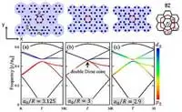
 the corresponding photonic bands")
Pic: (Top) Schematic of photonic crystals consisting of nanorods derived from the honeycomb lattice viewed from above, and (bottom) the corresponding photonic bands.
Author
Peggy Lee
Source: www.newelectronics.co.uk
 A new class of metals, revealed by researchers at Princeton, Yale, and the University of Zurich, possesses electronic properties that could help scientists find other, similarly-endowed materials.
The study described the class of metals based on their symmetry and a mathematical classification known as a topological number, which is predictive of special electronic properties.
"Topological classification is a very general way of looking at the properties of materials," said Princeton graduate student Lukas Muechler.
"The idea is that you don't really care about the details. As long as two materials have the same topological invariants, we can say they are topologically equivalent.”
While searching for superconductivity in a crystal of WTe2, a neighbouring lab instead found that the material could continually increase its resistance in response to magnetic fields.
The team extended the neighbouring labs’ research by considering the arrangement of the atoms in the crystal. While WTe2 is composed of many layers of atoms stacked upon each other, the team found that a single layer of atoms had a particular nonsymmorphic symmetry.
Having established the symmetry, the researchers mathematically characterised all possible electronic states having this symmetry, and classified those states that can be smoothly deformed into each other as topologically equivalent.
From this classification, they found WTe2 belongs to a new class of metals which they coined nonsymmorphic topological metals. These metals are characterised by a different electron number than the nonsymmorphic metals that have previously been studied.
In nonsymmorphic topological metals, the current-carrying electrons behave like relativistic particles. According to the team, this property is not as susceptible to impurities and defects as ordinary metals, making them attractive candidates for electronic devices.
"The silicon in modern devices has to be extremely pure and cristalline which requires complex fabrication methods," explained Muechler. "One could imagine that in future devices these fabrication procedures could be simplified due to the robustness of the electronic states in these new materials towards external factors.
"Materials such as WTe2 could be used as switches or sensors. With no external magentic field, the resistivity of the materials is low. If one applies a magnetic field, the resisistivity increases by several orders of magnitude. One could use these properties to define 'on' and 'off' signals, depending on the resistivity of the sample."
Author
Peggy Lee
Source: www.newelectronics.co.uk
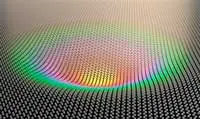 Researchers from TU Delft and Graphenea in Spain have found a way to create what they call 'mechanical pixels'. While the pixels, created using balloon like structures, do not emit light, they could be used in energy-efficient colour displays for a range of applications.
The 'pixels' are 13µm wide circular indents in silicon covered by a double layer of graphene, which encloses air inside the cavities.
When the researchers observed the pixels, they saw their colours were not constant. Dr Samer Houri, a researcher at TU Delft, led the work. “We observed Newton rings and noticed their colour changing over time,” he said. "It became clear the pixels were behaving like tiny balloons – in some, pressure differences caused the graphene membrane to be pressed downwards; in others, the membrane was pushed upwards."
The colour change is caused by interference between light waves reflected from the bottom of the cavity and the membrane on top. When the membranes are closer to the silicon, they appear blue. When the membranes are pushed away from the silicon, they appear red.
By applying a pressure difference across the graphene membranes, the perceived colour can be shifted continuously and researchers are working on a way to control the colour electrically.
PhD student Santiago Cartamil-Bueno said: “These devices provide a means to implement display technology based on interferometric modulation – or IMOD. By using graphene, an IMOD could improve device performance – including power consumption, pixel response time and failure rates – while enabling electrical integration and even flexible devices.”
The researchers hope to have developed a prototype ready for demonstration at Mobile World Conference in Barcelona.
Author
Graham Pitcher
Source: www.newelectronics.co.uk
 Researchers at the Moscow Institute of Physics and Technology believe it will be possible to predict accurately the level of noise caused by the amplification of photonic and plasmonic signals in nanoscale optoelectronic circuits. The scientists say their approach could be used not only to evaluate the ultimate data transfer rates in emerging optoelectronic devices, but also to discover the fundamental bandwidth limitations of nanophotonic interfaces.
The main obstacle faced by plasmonics is said to be signal attenuation. Due to high losses, surface plasmons can only propagate over long distances in active plasmonic waveguides. While these guide the plasmonic signal from the transmitter to the receiver, they also amplify it using the electrical energy flowing through the device. However, amplification also adds unwanted random signals – or noise.
Researcher Dmitry Fedyanin said: “Signal amplification inevitably decreases the signal-to-noise ratio and the more gain an amplifier provides – or, in our case, the greater the signal loss it needs to compensate for – the more noise it produces. This problem is especially pronounced in plasmonic waveguides with gain.”
Because noise causes errors during transmission, it reduces the effective data transfer rate due to the need for error correction. Error control also requires additional on-chip components, making new devices more difficult to design and manufacture.
"If we know the noise power in a nanophotonic communication channel, as well as its spectral characteristics, it is possible to evaluate the maximum data transfer rate along that channel,” researcher Andrey Vyshnevyy pointed out. “Furthermore, we can identify ways to reduce noise by choosing certain regimes of device operation and by using optical and electrical filtering techniques."
The theory targets a new class of device, which combines the advantages of electronics and photonics. In such a chip, plasmonic components would be used for ultrafast communication between processor cores and registers. Although signal attenuation was previously regarded as the proposed chip's main drawback, the Russian study shows that, as soon as the loss of signal has been compensated, a way must be found to deal with noise. If not, the signal might get drowned by spontaneous emissions, making the chip virtually useless.
The researchers’ calculations are said to show that an active plasmonic waveguide with a cross section of 200 × 200nm could be used to transmit signals over a distance of 5mm at more than 10Gbit/s per spectral channel.
Concluding, they believe it will be possible to create a device which combines miniature size and low error count with high data transfer rates and relatively high energy efficiency. And this ‘plasmonic breakthrough’ could come in the next 10 years.
Author
Peggy Lee
Source: www.newelectronics.co.uk