
Electronics News
Archive : 8 February 2017 год
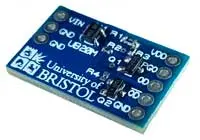 A low-cost chip developed at the University of Bristol is said to extend battery life in sensors; in some cases, by more than 10 times. The patent pending UB20M voltage detector is a ‘keep-alive’ device which, when combined with a suitable sensor, is said to eliminate standby power by enabling zero-power sensing and listening.
The developers say the device will allow designers to create circuits that can perform continuous monitoring without using battery power and to implement wireless wake-up with zero receiver power. Requiring no power supply, the chip uses a fraction of the power in the sensor’s output signal.
Dr Bernard Stark, from the Bristol Electrical Energy Management Research Group, said: “The UB20M provides sensing that is continuous and free. This is because it is able to respond to minute quantities of power from unpowered sensors. No battery or other power is needed for the device to stay alive and listening and battery maintenance is therefore reduced or not needed. We are now actively seeking commercial partners to use the voltage detector chip in their product.”
According to the team, the voltage detector uses more than 1000 times less energy than existing detectors to create a turn-on signal – 5pJ from around 0.5V. Because many sensors can provide this, listening is effectively free.
Potential applications are said to include: battery-driven sensors and monitoring systems; remotely-powered sensors; the elimination of mechanical switches; and the generation of sensing data only when useful data is available.
Author
Graham Pitcher
Source: www.newelectronics.co.uk
 Imec, Holst Centre and Rohm have described an all-digital phase-locked loop (ADPLL) for IoT radio transceivers at ISSCC 2017 in San Francisco.
According to the partners, a PLL is not only one of the major power consumers in a radio, but can also take up to 30% of the radio area. In contrast, the ADPLL occupies just 0.18mm2 in a 40nm CMOS process and consumes 0.67mW while performing better than digital PLLs.
PLLs have traditionally been analogue components, although researchers have been developing digital alternatives. ADPLLs, the partners assert, enable a smaller footprint, better control and testability and improved scaling to advanced CMOS nodes, but their performance has lagged that of analogue solutions.
Supporting all Bluetooth Low Energy specifications while reducing cost and power consumption to less than any comparable solution, the dividerless fractional-N digital PLL is said to feature power-efficient spur-mitigation and digital phase unwrap techniques.
Kathleen Philips, imec/Holst programme director, noted: “The ADPLL is ready for industrial mass production and is currently being transferred to our industrial partners for product integration.”
Author
Graham Pitcher
Source: www.newelectronics.co.uk
 imec, Holst Centre and Cartamundi claim to have demonstrated the first thin film tag on plastic, compatible with the near field communication (NFC) barcode protocol – a subset of ISO14443-A – which is available as a standard in many commercial smartphones.
“Making a plastic electronics device compatible to the ISO standard originally designed for silicon CMOS was a challenging research and development expedition,” stated Kris Myny, senior researcher at imec.
The NFC tag is manufactured with a thin film transistor technology using indium gallium zinc oxide thin film transistors (IGZO TFT) on a plastic substrate.
“This hardware solution of plastic NFC tags opens up several new possibilities for NFC deployments,” said Alexander Mityashin, program manager at imec.
“Thanks to the nature of thin film plastics, the new tags can be made much thinner and they are mechanically robust. Moreover, the self-aligned IGZO TFT technology offers manufacturing of chips in large volumes and at low cost.”
The IGZO TFT technology uses large-area manufacturing processes that allow for inexpensive production in large quantities, which makes it suitable for plastic electronics that requires a continuous supply of countless disposable devices.
The researchers developed a self-aligned TFT architecture with scaled devices optimised for low parasitic capacitance and high cut-off frequency. This allowed design of a clock division circuit to convert incoming 13.56MHz carrier frequency into system clock of the plastic chip.
Optimisations at logic gate and system level reduced power consumption down to 7.5mW, enabling readout by commercial smartphones.
Author
Peggy Lee
Source: www.newelectronics.co.uk
 Self-reinforcing solitary wave packets called solitons could achieve a more stable transmission of information, according to scientists at the Centre for Artificial Low Dimensional Electronic Systems (CALDES), within Korea's Institute for Basic Science (IBS). Their experiments and models are said to pave the way to a new field of electronics: solitonics.
A similar concept to topology could be used in IT to protect the flow of information from external interferences and impurities and guarantee its stability over longer distances and time. Until now however, the transmitted information was too stable to be modified and used.
One of the key components of the physics of topological system is the soliton, a stable solitary wave packet of energy, which travels though some 1D materials without losing its shape and energy.
The scientists explored the properties of solitons on a double chain of indium atoms placed on the top of a silicon surface and claim to have found that solitons could exist in three forms.
"In a topological sense, it is like having a donut with a lot of holes, where each hole can be of three different shapes corresponding to the three types of solitons," explained researcher Yeom Han Woong.
In this study, the team observed that solitons can be transformed and yet remain immune to the defects of the medium.
"So far solitons could only be created or destroyed in pairs, no other manipulations were possible, but we showed that these solitons can be switched from one to another, and even used for logical operations,” continued Woong.
These three types of solitons can also be represented by digits which can then be used for mathematical computations.
IBS scientists envisage new generation IT devices that combine silicon and solitons. "We are using solitons travelling in indium atoms on a silicon surface, and we imagine that this structure that could be implemented in current silicon devices, creating hybrid systems," concluded researcher Kim Tae-Hwan.
Author
Peggy Lee
Source: www.newelectronics.co.uk
 In a move which it claims sets the standard for precision amplifiers, Texas Instruments has launched the OPA388, which it describes as the first operational amplifier to offer zero-drift and zero-crossover technology.
This, it continues, allows the device to maintain high precision across the entire input range in such applications as test and measurement, medical and safety equipment and high-resolution data-acquisition systems. Ying Zhou, marketing manager for precision amplifiers, said: “Op amps have to deal with different sensors, such as temperature and pressure, so need high precision. They also need low noise and existing products either have too much noise or not enough bandwidth.”
The OPA388’s architecture offers high input linearity and precision. Zero drift eliminates temperature drift and flicker noise, while the zero-crossover topology eliminates offset errors caused by common-mode limitations.
Zhou pointed out: “The architecture minimises 1/f noise. With some amps, this can be 100nV/√Hz; this device is less than 10nV/√Hz over frequencies ranging from 1 to 10kHz, so it’s good for small sensor signals.”
Zero crossover functionality is enabled by an internal 1.8V charge pump. “Traditionally, zero crossover is implemented using P and N channel devices to get rail to rail operation. However, in the transition between the two, the voltage might jump or change quickly,” Zhou explained. “The charge pump gives a linear output with almost no harmonics.”
With a 10MHz gain bandwidth product, the part has a total harmonic distortion of -132dBc and an open loop gain of 148dB.
Author
Graham Pitcher
Source: www.newelectronics.co.uk