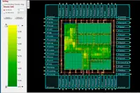
 Cadence Design Systems has introduced the Innovus Implementation System, said to allow SoC developers to improve power, performance and area (PPA), while reducing time to market. According to the company, Innovus can improve PPA by up to 20% at advanced process nodes and is '10nm ready'.
Key features of the package include:
• GigaPlace solver-based placement technology
• Advanced timing and power driven optimisation
• Concurrent clock and datapath optimisation
• Next generation slack driven routing with track aware timing optimisation
• Multi objective technology for global optimisation
Core algorithms have been upgraded with multithreading whilst a massively distributed parallel solution enables design blocks with 10million instances or larger. Multi scenario acceleration is said by Cadence to speed runtime, even with more multimode, multi corner scenarios.
"Customers have already started to employ the Innovus Implementation System to help achieve higher performance, lower power and minimised area to deliver designs to the market before the competition," said Anirudh Devgan, senior vice president of Cadence's Digital and Signoff Group. "Early customers are reporting significantly better PPA and a substantial speed up in turnaround time reduction versus competing solutions."
In a testimonial supplied by Cadence, Fares Bagh, vice president, hardware and architecture engineering with Freescale's Digital Networking Group, said: "We've tested the full Innovus Implementation System flow on some of our most congestion challenged 28nm networking IP blocks and have achieved excellent results while seeing significant throughput improvements
"The solution has enabled us to resolve our most difficult timing requirements and we anticipate that our deployment will allow us to grow our IP block sizes and accelerate SoC level design closure."
Key features of the package include:
• GigaPlace solver-based placement technology
• Advanced timing and power driven optimisation
• Concurrent clock and datapath optimisation
• Next generation slack driven routing with track aware timing optimisation
• Multi objective technology for global optimisation
Author
Graham Pitcher
Source: www.newelectronics.co.uk

